Why Is Via Placement Crucial in 4-Layer PCB Design?
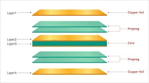
Designing a 4-layer Printed Circuit Board (PCB) involves a delicate balance of performance and cost, commonly featuring two external signal layers and two internal layers typically designated for power and ground planes. This architecture significantly improves signal integrity and power distribution compared to simpler 2-layer boards. However, the precise placement of vias—small conductive pathways connecting different layers—is paramount. Incorrectly positioned vias can introduce signal noise, create impedance mismatches, and disrupt stable power delivery, thereby compromising the board's overall functionality.
Strategic via placement is essential for minimizing signal loss, mitigating electromagnetic interference (EMI), and ensuring a consistent and stable power supply across the board. This guide delves into best practices for optimizing via placement in 4-layer PCBs, focusing on strategies that enhance both signal and power delivery for reliable and efficient electronic designs.
What Are the Different Types of Vias Used in 4-Layer PCBs?
Understanding the various via types is fundamental before delving into placement strategies, as each serves a distinct purpose and impacts signal and power delivery differently within a 4-layer PCB structure.
Through-Hole, Blind, and Buried Vias
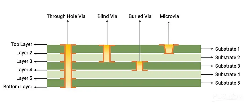
Through-Hole Vias extend completely through all layers of the PCB, connecting traces or components from the top to the bottom. While straightforward to manufacture, they can occupy valuable space on internal layers and potentially introduce unwanted capacitance, which may affect high-speed signals.
Blind Vias connect an outer layer to an internal layer without penetrating the entire board. For example, a blind via might link the top signal layer to an internal ground plane. They are effective for conserving space but generally incur higher fabrication costs due to their precision manufacturing.
Buried Vias are exclusively used to connect internal layers, remaining hidden from the outer surfaces of the PCB. These are beneficial for routing signals or power between internal planes but also contribute to increased manufacturing expenses.
Microvias for High-Density Applications
Microvias are significantly smaller vias, predominantly used in high-density interconnect (HDI) designs. They typically connect only adjacent layers and are critical for minimizing signal path lengths in applications where high-speed signals require the shortest possible routes to preserve integrity. The selection of via types hinges on specific design needs, such as signal speeds, component density, and budget constraints. For most 4-layer PCBs, a pragmatic approach often involves combining through-hole and blind vias to achieve an optimal balance between cost and performance.
How Does Via Stitching Improve 4-Layer PCB Performance?
Via stitching is a crucial technique in 4-layer PCB design, aimed at robustly connecting ground or power planes across different layers. This practice significantly enhances both electrical and thermal performance, particularly by creating a low-impedance path for current return and effectively reducing electromagnetic interference (EMI).
Benefits and Strategic Placement of Stitching Vias
Why Stitching Matters: In a 4-layer board where internal layers are often dedicated to power and ground, stitching vias ensure a consistent and stable reference potential throughout the board. Without proper stitching, high-frequency signals can induce ground bounce, create unwanted ground loops, or cause significant voltage drops, leading to signal degradation and noise. Moreover, stitching vias play a vital role in thermal management by providing multiple pathways for heat to dissipate, thus improving the thermal profile of the PCB.
Best Practices for Implementation:
● Strategically place stitching vias along the perimeter of the PCB to form a "via fence." This acts as an effective shield, helping to contain EMI within the board and prevent external interference.
● Position these vias near high-current components or areas characterized by significant switching activity to effectively minimize localized voltage fluctuations and maintain power stability.
● For optimal performance, space stitching vias at intervals approximately 1/20th of the wavelength of the highest frequency signal present on the board. For example, with a 1 GHz signal, this equates to roughly 15 mm, though precise spacing can vary based on the dielectric properties of the PCB material.
● Employ a grid-like pattern for stitching vias across expansive ground planes to guarantee a uniform distribution of current and prevent localized impedance spikes.
Managing Impedance Control with Vias in 4-Layer PCBs
Achieving consistent impedance is paramount for high-speed signals in 4-layer PCBs. Any impedance mismatch introduced by vias can lead to undesirable signal reflections, increased crosstalk, and potential data errors, particularly in circuits operating at higher frequencies.
How Vias Influence Impedance
A via inherently acts as a complex combination of a small inductor and capacitor within the signal path. This alters the characteristic impedance of the trace, causing discontinuities. For instance, a 50-ohm microstrip trace might see its impedance increase to 60 ohms or more when passing through a poorly designed via, resulting in signal reflections. This effect becomes significantly more pronounced at higher frequencies, typically above 500 MHz, where even minor discontinuities can have a substantial impact on signal integrity.
Techniques for Effective Impedance Control with Vias
To maintain consistent impedance when signals transition through vias:
● Minimize Via Length: For high-speed signals, prioritize the use of blind or microvias. Shorter vias inherently possess less inductance, which helps to keep the impedance closer to the target value and reduces reflections.
● Ensure Ground Return Paths: Always place a dedicated ground via in close proximity to each high-speed signal via. This provides an immediate and low-inductance return path for the signal current, critical for preserving signal integrity and minimizing loop inductance. A common guideline suggests placing a ground via within 0.5 mm of its corresponding signal via.
● Limit Via Transitions: Avoid routing high-speed signals through multiple vias whenever possible. Each layer transition introduces an additional impedance discontinuity, compounding the risk of reflections and signal degradation.
● Utilize Simulation Tools: Integrate simulation tools into the design phase to accurately model via impedance. These tools allow designers to experiment with adjustments to via diameter (e.g., reducing from 0.3 mm to 0.2 mm) or pad size to fine-tune impedance matching with the adjacent traces.
Suggested Reading: Designing with Four-Layer PCBs: A Comprehensive Guide
Optimizing Power Via Placement for Stable 4-Layer PCBs
Stable power delivery is a foundational element of any robust PCB design. In a 4-layer configuration, power vias are responsible for connecting components to the internal power planes. Suboptimal placement of these vias can lead to significant voltage drops, increased noise, and inefficient power distribution, directly impacting overall board reliability.
Strategic Considerations for Power Via Placement
Thoughtful placement of power vias is essential for maintaining a clean and stable power supply:
● Proximity to Components: Position power vias as close as possible to the power pins of integrated circuits (ICs) and other high-current drawing devices. This minimizes the parasitic resistance and inductance in the power path, which is crucial for reducing localized voltage drops. For example, placing a via within 0.5 mm of a power pin can reduce the IR (voltage) drop by up to 10% in certain designs.
● Decoupling Capacitor Integration: Ensure power vias are placed in immediate proximity to decoupling capacitors. This arrangement creates a low-impedance connection from the capacitor to the power plane, allowing it to effectively supply transient currents. A common practice is to place a via on each side of the capacitor pad, connecting directly to the power and ground planes.
● Appropriate Via Sizing: Select larger diameter vias for power connections, as these can handle higher current loads more effectively. While a 0.4 mm diameter via might typically carry 1-2 A, it's vital to consult your online PCB manufacturer for specific current limits based on copper thickness (e.g., 1 oz or 2 oz).
● Multiple Vias for High Current: For components that draw substantial current, such as power regulators or FPGAs, consider employing multiple power vias in parallel. This strategy significantly reduces the effective resistance of the power path and enhances thermal dissipation, preventing localized hot spots.
How Does Signal Via Placement Impact 4-Layer PCB Integrity?
Signal vias are fundamental for routing traces between layers, especially for high-speed or critical signals within a 4-layer PCB. Inaccurate placement can severely degrade signal quality, particularly for frequencies exceeding 100 MHz, leading to issues like signal loss and increased noise.
Best Practices for Signal Via Placement
Implementing these strategies will help preserve signal integrity across layer transitions:
● Shortest Possible Path: Always strive to create the shortest possible path when transitioning signals between layers. For example, if a signal needs to move from the top layer to an internal signal layer, using a blind via is preferable to a through-hole via to minimize unnecessary trace length and inductance.
● Dedicated Return Path: It is critical to provide a nearby ground via for every signal via. This ensures a consistent and low-inductance return path for the signal current. Without an adjacent return path, the signal current may be forced to couple to unintended planes or traces, significantly increasing crosstalk and EMI. A spacing of 0.3-0.5 mm between signal and ground vias is often sufficient.
● Mitigating Stub Effects: Unused portions of through-hole vias, known as stubs, can act as resonant antennas, causing unwanted signal reflections, particularly at high frequencies. If through-hole vias are unavoidable for high-speed signals, consider back-drilling to remove the unused stub or opt for blind vias as an alternative.
● Adequate Spacing Between Signals: Maintain sufficient clearance between high-speed signal vias to prevent unwanted coupling and crosstalk. A general guideline is to space signal vias at least 2-3 times the via diameter apart. For instance, with a 0.25 mm via, a spacing of 0.5-0.75 mm would be appropriate.
Common Pitfalls to Avoid in 4-Layer PCB Via Design
Even experienced designers can encounter issues with via placement. Recognizing and avoiding these common mistakes can save significant time and resources during the PCB development cycle.
Overlooking Key Design Principles
● Excessive Use of Through-Hole Vias: Relying solely on through-hole vias can lead to cluttered internal layers and unnecessary disruptions in power and ground planes. Prioritize the use of blind or buried vias where design complexity and budget allow, as they offer more efficient space utilization.
● Neglecting Thermal Management: Vias carrying high currents can generate localized heat if not adequately sized or surrounded by sufficient copper. Ensure that high-current vias are appropriately sized and have ample copper heatsinking to dissipate heat effectively, preventing thermal hotspots and potential component damage.
● Skipping Simulation and Verification: Failing to simulate the impact of vias on impedance control, power delivery networks, or signal integrity can result in unforeseen performance issues during board testing. Employ design tools to model via effects and validate placement strategies before committing to fabrication.
● Inadequate Spacing Between Vias: Placing vias too closely together can lead to manufacturing defects, such as shorts, or create undesirable signal coupling. Always adhere to your PCB manufacturer's design rules for minimum via spacing, which is often around 0.2-0.3 mm for standard fabrication processes.
Concluding Thoughts on Mastering Via Placement for 4-Layer PCBs
Effective via placement in 4-layer PCBs is a fundamental skill for optimizing both signal and power delivery, directly impacting the board’s overall performance and reliability. Every decision—from selecting the appropriate via types to implementing advanced stitching techniques, meticulous impedance control, and strategic positioning of power and signal vias—plays a critical role in the final outcome. By diligently following the best practices outlined in this guide, designers can significantly mitigate noise, reduce electromagnetic interference (EMI), and ensure exceptionally stable operation for their electronic designs.
It is crucial to remember that while these guidelines offer a robust framework, each project presents unique requirements. Therefore, adapting these principles to suit your specific application is key to success. With thorough planning and meticulous attention to detail in your via placement strategies, your 4-layer PCB designs can achieve the high levels of reliability and efficiency demanded by today’s advanced electronic applications. Incorporate these insights into your next design endeavor and observe a notable improvement in your PCB performance.


