Introduction
Heavy copper PCBs carry 3 oz/ft² (105 µm) or thicker copper layers, with many industrial designs reaching 6–20 oz (210–700 µm) on outer layers and even higher on inner layers. These boards serve motor drives, inverters, traction systems, renewable energy converters, and industrial power supplies where currents routinely exceed 50–500 A. Proper heavy copper PCB design ensures reliable current carrying, effective thermal management, and long-term mechanical stability under high-power conditions.
Why Heavy Copper Becomes Necessary in Power Electronics
Standard 1–2 oz copper limits safe continuous current to roughly 5–12 A per millimeter of trace width at 30 °C temperature rise. Industrial applications frequently demand 100–1000 A in compact footprints. Increasing copper thickness directly reduces I²R losses and voltage drop while lowering operating temperature for the same current.
Heavy copper also improves heat spreading across the board plane, reducing hot spots under high-power components such as IGBT modules, MOSFETs, and bus capacitors.
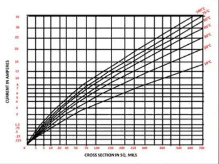
Current-Carrying Capacity According to IPC-2152
Designers must base trace width calculations on IPC-2152 (Conservative Standard for Determining Current-Carrying Capacity in Printed Board Design). The standard provides charts and equations for external and internal layers at different copper weights and acceptable temperature rises.
Example values from IPC-2152 (10 °C rise, external layers, no plane):
| Copper Weight | Trace Width for 100 A | Trace Width for 200 A | Trace Width for 300 A |
|---|---|---|---|
| 3 oz (105 µm) | 10.2 mm | 23.5 mm | 41.0 mm |
| 6 oz (210 µm) | 4.8 mm | 10.5 mm | 17.8 mm |
| 10 oz (350 µm) | 2.7 mm | 5.9 mm | 10.0 mm |
| 20 oz (700 µm) | 1.3 mm | 2.8 mm | 4.7 mm |
Thermal Management Strategies in High-Power PCBs
Copper Thickness and Plane Thermal Resistance
Thermal conductivity of copper remains ~390 W/m·K regardless of thickness. Increasing thickness proportionally reduces in-plane thermal resistance. A 10 oz copper plane spreads heat far more effectively than 2 oz, lowering component junction temperature by 15–40 °C in typical power converter layouts.
Via Arrays and Thermal Vias
Heavy copper PCB often use via-in-pad or large thermal via arrays filled with copper or conductive epoxy to move heat from top-side components to inner or bottom copper planes. IPC-6012E Class 3 requires minimum 25 µm copper plating in thermal vias when filled and planarized.
Metal-Backed and IMS Substrates
When board-plane spreading alone proves insufficient, designers combine heavy copper FR-4 multilayers with direct-bonded aluminum or copper baseplates (IMS). The dielectric layer in IMS typically provides 1–3 W/m·K through-plane conductivity.
Key Design Rules for Reliable Heavy Copper PCBs
Minimum Annular Ring and Drill-to-Copper Clearance
IPC-2221B and IPC-6012E require increased annular ring for thick copper because plating aspect ratio becomes challenging above 6 oz.
Recommended minimum values (Class 3):
| Copper Weight | Minimum Annular Ring (finished) | Minimum Drill-to-Copper Clearance |
|---|---|---|
| 3–6 oz | 0.20 mm | 0.30 mm |
| 7–12 oz | 0.25 mm | 0.40 mm |
| 13–20 oz | 0.30 mm | 0.50 mm |
Etch Compensation and Trapezoidal Trace Profile
Thick copper etches with significant undercut, creating trapezoidal cross-sections. Design software must apply etch compensation (typically 0.075–0.15 mm per side depending on copper thickness) to achieve target final width at the trace bottom.
Solder Mask and Silkscreen Considerations
Liquid photoimageable (LPI) solder mask thickness increases over heavy copper features. Standard 20–30 µm LPI may leave insufficient coverage on 400–700 µm steps. Many facilities apply double-pass solder mask or use dry-film mask for better step coverage.
Resin Fill and Planarization
Deep cavities between thick copper creates after etching require non-conductive epoxy fill and surface planarization before solder mask application. IPC-6012E section 3.6.2.13 specifies maximum 75 µm surface topography after planarization for Class 3 products.
Suggested Reading: Heavy Copper PCB: An overview of its benefits and applications
Mechanical Stress and Reliability Considerations
Thicker copper increases CTE mismatch stress on plated through-holes during thermal cycling. IPC-TM-650 2.6.8 (Thermal Stress Test) and IPC-9701A (Performance Test Methods) qualify heavy copper boards with 6× reflow at 260 °C followed by −40 °C to +145 °C thermal cycling.
Common mitigation techniques:
- Use of high-Tg material (≥170 °C) and low-CTE laminates
- Tear-drop pads at hole entrances
- Anchor spurs on large copper features
- Back-drilling or controlled-depth drilling for thick boards (>4.0 mm)
Layout Best Practices for Power Electronics PCBs
- Route high-current paths first using maximum available copper weight
- Keep trace lengths as short as possible to minimize inductance
- Use multiple parallel vias when transitioning between layers
- Place decoupling capacitors as close as possible to IC power pins
- Provide solid copper pours connected to chassis ground for EMI shielding
- Maintain symmetric stack-up to minimize bow and twist (IPC-6012E limits 0.75 % max)
Conclusion
Heavy copper PCB design transforms high-power industrial applications from thermal- and current-limited to reliable, compact, and efficient. Success depends on strict adherence to IPC-2152 for current capacity, IPC-6012E for fabrication limits, and IPC-2221B for generic design requirements. When copper thickness, thermal vias, resin planarization, and mechanical reliability receive proper engineering attention from the layout stage, the resulting boards deliver decades of field service in demanding motor drives, renewable energy systems, and traction converters.
FAQs
Q1: What are the benefits of heavy copper PCBs in aerospace applications?
A1: Heavy copper PCBs handle high currents up to 100A with superior thermal management in power PCBs, reducing hotspots 20°C per DO-160. Ideal for cockpit displays, they boost reliability in vibrations up to 20G.
Q2: How does power layer design impact high current PCBs in avionics?
A2: Power layer design in high current PCBs uses 4-6 oz Cu for <100 mV drops at 50A, per IPC-2221B. In aerospace, it isolates 400 Hz AC, ensuring stable feeds for displays without EMI.
Q3: What role does thermal management play in power PCBs for aircraft?
A3: Thermal management in power PCBs via vias and metal cores keeps junction temps <85°C in -40°C to 70°C swings. For cockpits, it prevents dimming, aligning with MIL-STD-704 surges.
Q4: How to meet aerospace power requirements with heavy copper PCBs?
A4: Heavy copper PCBs satisfy aerospace power requirements like 28V DC/400 Hz AC via thick planes and stitching, per DO-160G. They endure ±80V transients, vital for reliable cockpit avionics.
Q5: What trends affect heavy copper PCBs in 2025 cockpit displays?
A5: 2025 sees 48V adoption and embedded cooling in heavy copper PCBs, growing aero market to $2.8B. HDI hybrids enhance thermal management for AR-integrated displays.
References
IPC-2221B — Generic Standard on Printed Board Design. IPC, 2003.
MIL-STD-704F — Aircraft Electric Power Characteristics. U.S. Department of Defense, 2004.
DO-160G — Environmental Conditions and Test Procedures for Airborne Equipment. RTCA, 2010.
RTCA/DO-254 — Design Assurance Guidance for Airborne Electronic Hardware. RTCA, 2000.
Aerospace PCB Design Tips for Efficient Thermal Management. ProtoExpress, Mar 30, 2023.
J-STD-001 — Requirements for Soldered Electrical and Electronic Assemblies. IPC/JEDEC, 2020.
IPC-4101E — Specification for Base Materials for Rigid and Multilayer Printed Boards. IPC, 2010.
Thermal Management: Designing Aircraft Avionics Cooling Systems. Altium, Mar 22, 2021.
IPC-TM-650 — Test Methods Manual. IPC, 2023.
Aerospace PCB Assembly Basics. PCBASIC, Jan 16, 2025.
Design Issues on Thick/Heavy Copper PCBs for Military and Aerospace. PCBCart, undated.
Overview of MIL-STD-704 Requirements for Power Supply. Viable Power, undated.