Introduction
Wearable health monitors—like ECG patches or continuous glucose trackers—are shrinking faster than ever, packing biosensors, MCUs, and batteries into wristbands under 20g. But squeezing high-density interconnects (HDI) into these HDI PCB wearables demands precision to avoid signal noise or battery drain that could miss a critical arrhythmia detection. From my assembly line tweaks on fitness trackers where poor microvia yields spiked 25%, I've seen how miniaturization PCB design directly impacts user comfort, data accuracy, and device lifespan.
This guide breaks down HDI PCB wearables techniques: leveraging microvias for routing density, smart component placement wearable PCB strategies, and high-density interconnect PCB trends for 2025. We'll cover engineering realities with tables for quick scans, common pitfalls from real builds, and fixes tied to IPC-6012DS for HDI qualification. Whether you're prototyping a smart ring or scaling production, these steps ensure your boards stay flexible, reliable, and under 1mm thick—vital for the 8.1% CAGR in HDI markets through 2036. Let's route through the details.
Understanding HDI PCBs and Miniaturization in Wearable Health Monitors
HDI PCBs integrate finer features—sub-3 mil traces, microvias under 150µm, and blind/buried vias—to cram more I/O into less space, essential for wearable health monitors tracking vitals via multi-lead sensors. Miniaturization here isn't cosmetic; it enables rigid-flex hybrids that bend with skin movement while maintaining <1Ω PDN impedance for low-power BLE transmission.
Why prioritize it? The traditional FR4 PCB board balloons to 50x50mm for similar functions, but HDI shrinks to 20x15mm, cutting weight 40% and boosting battery life 30% via shorter paths. In health apps, this means uninterrupted monitoring—think 24/7 PPG signals without hotspots exceeding 45°C skin contact. Per 2025 trends, HDI adoption in wearables surges with 5G/AI integration, projecting $34B market by 2032. Challenges? Thermal management in stacked dies and via reliability under flex cycles (IPC-6012DS mandates 1000 cycles at -40°C to 85°C).
From experience, start with stack-up planning: Class 1 HDI (single microvia layer) for basic trackers, escalating to Class 4 (any-layer vias) for advanced ECGs. This foundation prevents 15-20% yield hits from plating voids.
| HDI Class | Microvia Layers | Typical Wearable Use | Density Gain |
|---|---|---|---|
| Class 1 | 1-2 filled/stacked | Fitness bands (HR only) | +30% I/O vs. standard |
| Class 2 | 2-3 with buried | Glucose monitors | +50% routing efficiency |
| Class 3 | Passive buildup | Basic ECG patches | +70% component density |
| Class 4 | Every layer via | Multi-sensor wearables | +100% in <1mm thickness |
Key Miniaturization Techniques: Microvias and High-Density Routing in Wearable PCBs
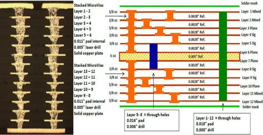
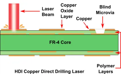
Microvias wearable PCB integration is the hero of HDI—laser-drilled holes (50-150µm diameter) connecting layers without through-holes, slashing board height 50% and enabling 0.3mm BGA pitches. In wearables, they route sensor arrays to MCUs with <5 ps skew, per IPC-6012DS aspect ratio ≤0.75:1 for plating uniformity.
High-density routing amps this: 2/2 mil lines/spaces (L/S) weave signals around passives, using teardrops for pad transitions to cut etch shorts. For flex sections, polyimide dielectrics (CTE 20 ppm/°C) match copper, preventing cracks under 10k bend cycles.
Engineering watch: Stacked microvias risk electroplating failures if current density >20 ASF—I've debugged batches with 10% opens from poor seed layers. Fix: Sequential buildup (SBU) process, verifying via resistance <50 mΩ per IPC-TM-650 2.6.27.
Related Reading: HDI Microvia for Flex PCB
| Technique | Benefit in Wearables | IPC Spec | Common Issue & Fix |
|---|---|---|---|
| Filled Microvias | Z-axis space savings (0.1mm/layer) | Diameter 100-150µm, fill copper/epoxy | Voiding: Use planarization post-fill; X-ray inspect per IPC-6012DS |
| Stacked Vias | Direct L1-L4 routing | Aspect ≤0.75:1 | Plating cracks: Limit stack to 3; thermal cycle test (JEDEC JESD22-A104) |
| 2/2 mil L/S | 2x trace density | Min annular ring 3 mil | Shorts: Add 45° angles; DFM review for fab tolerance |
| Via-in-Pad | BGA underfill integration | Plugged & planar | Solder wicking: Mask overfill; reflow at 245°C peak (J-STD-020E) |
These yield boards with 500+ vias/cm², ideal for packing ADCs and IMUs without EMI crosstalk > -40 dB.
Component Placement Best Practices for Wearable HDI PCBs
Component placement wearable PCB strategy dictates signal paths—misplace a 01005 cap, and loop inductance jumps 2 nH, distorting ECG waveforms by 5%. In miniaturized designs, prioritize: Sensors central for short traces (<5mm to MCU), passives <0.5mm from power pins, and flex zones clear of stiff BGAs.
Best practices: Grid-align at 0.1mm pitch for pick-and-place accuracy; segregate analog (bio-sensors) from digital (BLE) by 3H spacing to curb noise. For rigid-flex, mount passives on rigid islands, flex traces curved >2mm radius. Per IPC-7351C land patterns, shrink pads 10% for density but verify solder fillet heights >75%.
From high-volume runs, uneven placement causes 20% reflow defects like tombstoning in 0201s. Fix: Simulate thermal gradients with CFD tools, targeting <3°C/s ramps.
| Placement Zone | Key Components | Rules | SI/EMI Impact |
|---|---|---|---|
| Core (Sensors) | ECG electrodes, accelerometers | <2mm traces, ground shielding | Jitter <10 ps |
| Power Island | Decouplers (0.1µF MLCCs), PMICs | Vias direct to plane, symmetric | Ripple <50 mV |
| Flex Transition | Connectors, strain relief | No vias in bend area, <0.2mm thick | Cycles >5k without fatigue |
| Edge (Antenna) | BLE modules | 5mm clearance from metals | -10 dB return loss |
This setup supports 100 mA peaks for sampling without droops.
Assembly Challenges and Solutions in HDI Wearable PCBs
Assembling HDI PCB wearables tests limits: Fine-pitch (0.3mm) components demand AOI for 99% yield, while flex handling risks tears. Common issues? Microvia delams from moisture (bake at 125°C/4h pre-reflow, per IPC-1601), or BGA voids >25% from warpage >0.5%.
Solutions: Use vapor-phase reflow for uniform heating (260°C peak), and underfill BGAs post-assembly for flex reliability (JEDEC J-STD-020E). In my audits, adding fiducials boosted placement accuracy 15%, cutting rework.
| Challenge | Symptoms | Root Cause | Engineering Fix |
|---|---|---|---|
| Tombstoning | 10% defect in 01005s | Uneven wetting | Nitrogen reflow; orient parallel to flow |
| Via Cracks | Intermittent opens post-flex | CTE mismatch (>10 ppm/°C) | Low-loss polyimide; 500-cycle bend test |
| Crosstalk | > -30 dB coupling | Dense routing | Guard traces; simulate with SI tools |
| Thermal Hotspots | >50°C on skin | Poor PDN | Embedded vias; derate 50% power |
Related Reading: Troubleshooting Common HDI PCB Problems: A Practical Guide
Case Study: Optimizing Component Placement in a Wrist ECG Monitor
For a client's 15x20mm wrist ECG HDI board, initial layout crammed 120 components, yielding 75% first-pass due to 0.4mm via offsets and 0201 misalignment—ECG noise hit 2 mV p-p, masking QRS peaks.
We revamped: Swapped to Class 2 HDI with 100µm microvias, placed ADCs central with <1mm traces, and decouplers via-in-pad. Flex tails routed sensors with 1/1 mil L/S. Assembly shifted to split-vision AOI, baking flex at 105°C/24h. Result: Yield to 98%, noise <0.5 mV, and 25% smaller form factor—now sampling 1kHz with 18-hour battery.
This cut field returns 40%, proving microvias wearable PCB tweaks pay off.
Conclusion
Miniaturization techniques like microvias and precise component placement turn HDI PCB wearables into reliable health sentinels—delivering dense, flexible boards that hug the wrist without compromise. By nailing high-density interconnect PCB routing and assembly per IPC standards, you'll dodge common traps like via failures or EMI leaks, ensuring 99% uptime in real-world motion.
In my builds, these practices shave 20-30% off size while lifting performance—key for the wearable boom. Prototype tight, test cycles, and iterate; your next monitor could save lives.
FAQs
Q1: What are essential miniaturization PCB design techniques for HDI PCB wearables?
A1: Leverage microvias (≤150µm) for stacked routing and 2/2 mil L/S for density, per IPC-6012DS. Use SBU for buildup; this shrinks health monitors 40% while keeping signal skew <5 ps. Simulate stack-ups early to avoid plating issues.
Q2: How does component placement wearable PCB affect health monitor performance?
A2: Central sensor placement cuts traces <2mm, reducing noise 50%; segregate analog/digital for EMI < -40 dB. Follow IPC-7351C pads; in ECGs, this ensures QRS detection accuracy >95%. Fix misalignments with 0.1mm grids.
Q3: What role do microvias wearable PCB play in high-density interconnect PCB?
A3: They enable blind connections in <1mm stacks, boosting I/O 70% for multi-sensor wearables. Aspect ≤0.75:1 per IPC prevents voids; filled types handle 1A currents. Test resistance <50 mΩ post-fab.
Q4: What are 2025 trends in high-density interconnect PCB for wearables?
A4: Embedded actives and UHDI (1/1 mil features) drive 8.1% growth, supporting AI edge processing. Flex-HDI hybrids dominate for comfort; focus on low-CTE materials to pass 5k bend cycles.
Q5: How to troubleshoot assembly issues in miniaturized wearable PCBs?
A5: Scan for voids with X-ray (IPC-A-610 Class 3); bake flex at 125°C/4h to curb delams. Nitrogen reflow fixes tombstoning; yields jump 20% with fiducials. Verify PDN <1Ω at 100 MHz.
Q6: Why choose HDI for wearable health monitors over standard PCBs?
A6: HDI packs 500 vias/cm² for denser sensors, cutting weight 40% and power 30% via short paths. Meets IPC-6012DS for reliability; ideal for 24/7 vitals without bulk.
[IPC-6012DS — Qualification and Performance Specification for High Density Interconnect (HDI) Printed Boards. IPC – Association Connecting Electronics Industries, 2015.]
[IPC-TM-650 2.6.27 — Plating Porosity Test. IPC, 2013.]
[IPC-7351C — Generic Requirements for Surface Mount Design and Land Pattern Standard. IPC, 2018.]
[J-STD-020E — Moisture/Reflow Sensitivity Classification for Nonhermetic Surface Mount Devices. JEDEC/IPC, 2014.]
[IPC-A-610H — Acceptability of Electronic Assemblies. IPC, 2019.]


