Used in inverters, servo drives, and high-power PLCs (Programmable Logic Controllers).
Handle higher currents, dissipate heat faster, and deliver unmatched reliability.


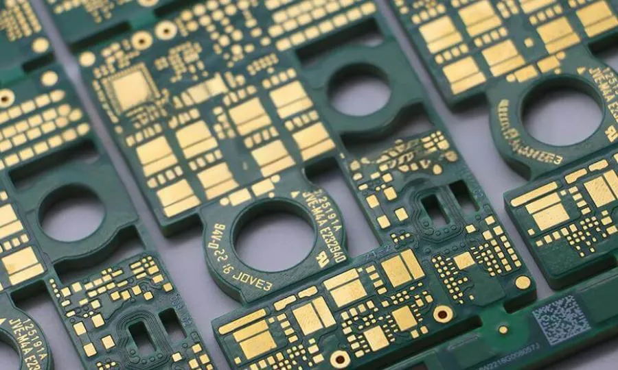
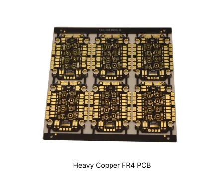
Heavy Copper PCBs are printed circuit boards manufactured with extra-thick copper layers (typically ≥3 oz/ft2, or over 105 μm) on substrates such as FR-4. Compared to standard PCBs (with 1–2 oz copper), heavy copper PCBs have significantly thicker copper layers, providing enhanced current-carrying capacity and thermal performance. They are widely used in new energy vehicles, high-power power supplies, industrial control systems, and other applications, making them the preferred choice for high-power, high-stability designs.
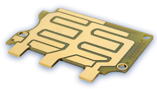
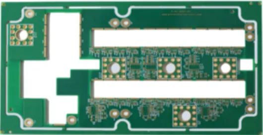
A 2-layer printed circuit board with relatively thick copper and ENIG (Electroless Nickel Immersion Gold)surface finish, widely used in the electronics industry.
Material: FR4 - TG180 / RoHS
Layers: 2
Board Thickness: 1.6 mm
Copper Thickness: 7 oz
Solder Mask / Silkscreen: Green solder mask / White silkscreen
Surface Finish: ENIG
Minimum Line Width / Spacing: 9 / 12 mil
Minimum Hole Diameter: 2.5 mm
Technical Feature: 7 oz copper
Designed for high-power, high-current, and high-heat-dissipation electronic applications.
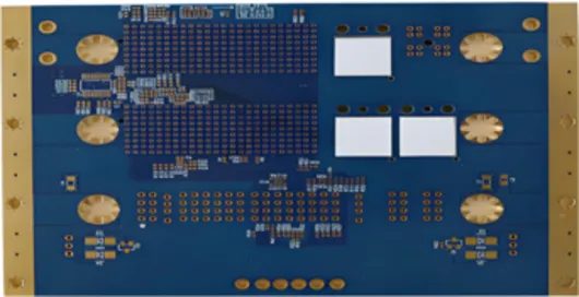
Material: FR-4
Layers: 4
Surface Finish: ENIG (Electroless Nickel Immersion Gold)
Minimum Drill Hole: 0.2 mm
Copper Thickness: 3 oz
Board Thickness: 1.6 mm
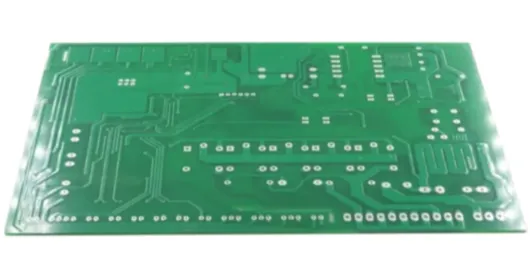
A 2-layer thick copper PCB designed for medical instruments where reliability and precision are critical.
Layers: 2
Minimum Line Spacing: 0.075 mm
Solder Mask: Blue
Standard: IPC-A-610 Class 2–3
Solder Mask Thickness: 20–50 μm
Minimum Hole Diameter: 0.2 mm
A key foundational component forindustrial control, automotive electronics, and energy equipmentapplications.
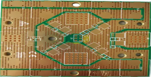
Material: Shengyi FR-4
Layers: 6
Surface Finish: ENIG (Electroless Nickel Immersion Gold)
Minimum Drill Hole: 0.3 mm
Copper Thickness: 3 oz
Board Thickness: 2.5 mm
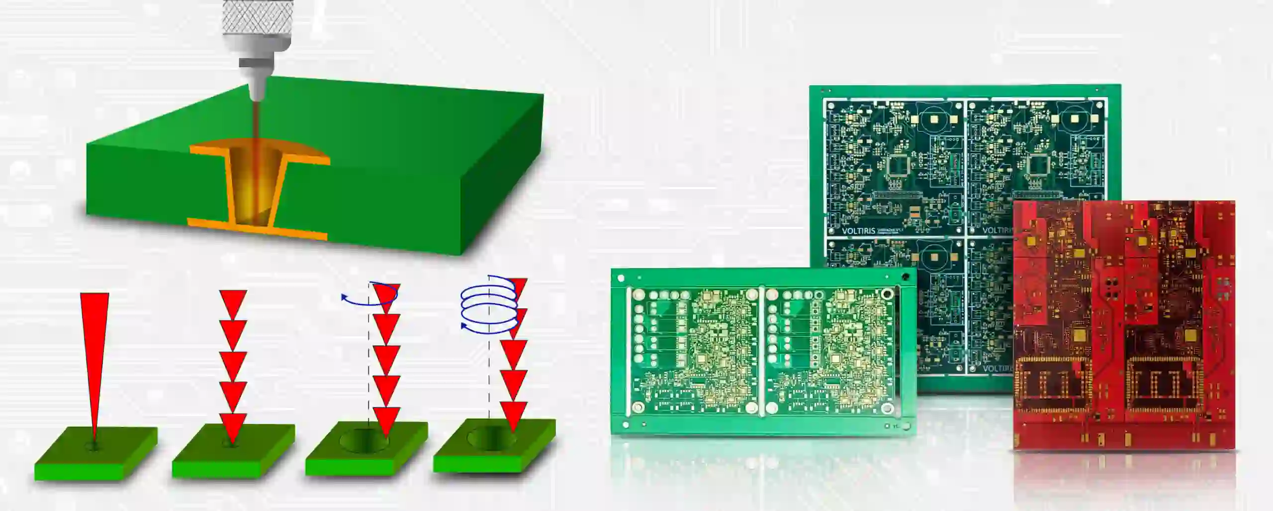
Thick copper layers can handle higher currents (e.g., tens of amperes in power modules), reducing resistive loss and the risk of overheating, and preventing circuit damage.
Copper's high thermal conductivity quickly transfers heat, lowering the operating temperature of electronic components and improving system stability and lifespan.
Heavy copper PCBs resist warping and delamination under repeated thermal cycles, ensuring long-term stability and reliability in power electronics, industrial, and aerospace applications.
Thick copper layers provide greater resistance to vibration and impact, making them suitable for harsh environments such as automotive and industrial equipment.
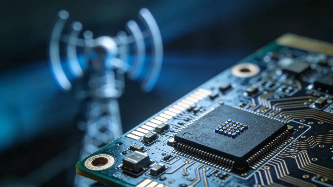
Reduces signal loss and crosstalk in high-frequency or microwave circuits, making it ideal for communication base stations, radar systems, and other high-frequency applications.
Can be fabricated using standard and advanced PCB techniques, including multi-layer lamination, SMT assembly, and precision etching, enabling complex circuit designs without compromising performance.
Used in inverters, servo drives, and high-power PLCs (Programmable Logic Controllers).

Applied in motor controllers, inverters, DC-DC converters, onboard chargers (OBC), and high-voltage distribution units (PDU).

Used in high-power LED streetlights, industrial and mining lamps, etc.
Applied in energy storage converters (PCS) and busbars for lithium battery energy storage cabinets.

Used in radar systems, communication modules, flight control units, and high-reliability avionics.

Used in railway control systems, electric vehicle inverters, motor controllers, and onboard power distribution units (PDUs).
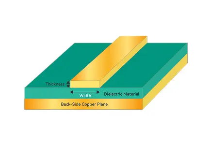
Key aspects of heavy copper construction include:
Thick Copper Layers: Provide high current carrying capacity and reduce resistive loss.
Robust Base Material: Ensures mechanical strength and dimensional stability.
Advanced Plating & Surface Finish: ENIG or HASL finishes protect the copper and ensure reliable soldering.
Thermal and Electrical Reliability: Optimized for industrial, automotive, military, and aerospace applications where high power and durability are required.
Heavy copper FR4 combines thick copper layers with standard FR4 materials to deliver high current capacity and improved thermal performance in power electronics.