PCB Specifications
| Parameter | Value | Parameter | Value |
|---|---|---|---|
| PCB Type | FR4 PCB | Quantity | 250 pcs |
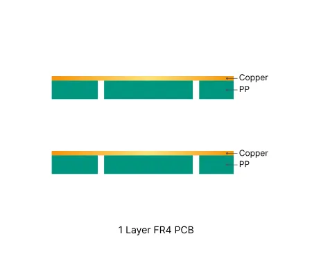
| Layers | 1 Layers | Board Type | Panel PCB |
| Dimensions | 210 x 272 mm | Copper Weight | 1oz |
| Thickness | 1.6 mm | Min Track / Spacing | 10/10mil |
| Surface Finish | HASL Lead Free | Min Hole Size | 0.8mm↑ |
| Solder Mask | Black | Silkscreen | White |
| Stack-up | Custom | Impedance Control | No |
Manufacturing Timeline
Logistics Information
Key Manufacturing Processes
Manufacturing Summary
This order consisted of 250 panels of single-layer FR4 PCB, each 210 × 272 mm with 1.6 mm thickness and 1 oz copper weight. The design used standard 10/10 mil trace width and spacing together with 0.8 mm minimum hole size, completed by black soldermask, white silkscreen, and HASL Lead Free finish on a custom stackup. These parameters required precise registration during material preparation to keep panel flatness within tolerance across the full quantity.
We executed circuit imaging and etching to define clean conductor patterns on one side, then applied soldermask before molten solder coating and hot air leveling. The chosen panel format simplified handling of the 210 × 272 mm size while maintaining edge clearance and avoiding mask encroachment on pads. Every step followed the established sequence for standard-geometry single-layer boards, ensuring uniform coating thickness on the HASL Lead Free surface.
Batch AOI inspection and electrical testing confirmed circuit continuity and solderability for all 250 panels. Production completed in 10.5 days with no rework required, delivering boards that matched the exact dimensions, finish, and silkscreen placement requested.
Explore More PCB Manufacturing Resources
Real Production Records
| Order ID | PCB Type | Layers | Dimensions | Solder Mask | Surface Finish | Quantity | Action |
|---|---|---|---|---|---|---|---|
| FR4-20260528-028 | FR4 PCB | 2 | 185 x 245 | Green | HASL Lead Free | 5 | View detail |
| FR4-20260526-001 | FR4 PCB | 2 | 100 x 100 | Green | HASL Lead Free | 10 | View detail |
| FR4-20260525-001 | FR4 PCB | 2 | 50 x 45 | Matte Green | HASL Lead Free | 20 | View detail |


