PCB Specifications
| Parameter | Value | Parameter | Value |
|---|---|---|---|
| PCB Type | FR4 PCB | Quantity | 10 pcs |
| Layers | 1 Layers | Board Type | Panel PCB |
| Dimensions | 146 x 219 mm | Copper Weight | 1oz |
| Thickness | 0.8 mm | Min Track / Spacing | 6/6mil↑ |
| Surface Finish | HASL Lead Free | Min Hole Size | 0.3mm↑ |
| Solder Mask | Green | Silkscreen | None |
| Stack-up | Default | Impedance Control | No |
Manufacturing Timeline
Logistics Information
Key Manufacturing Processes
Manufacturing Summary
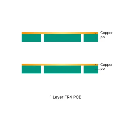
This order comprised ten single-layer FR4 panels measuring 146 × 219 mm with a board thickness of 0.8 mm and 1 oz copper weight. We applied standard 6/6 mil track and spacing along with 0.3 mm minimum holes, green solder mask, and HASL Lead Free surface finish while omitting silkscreen entirely. The reduced thickness required adjusted handling parameters during material preparation and imaging to preserve panel flatness and registration accuracy across the production run.
Execution followed a controlled sequence of circuit imaging and etching, solder mask application, molten solder coating, and hot air leveling. Process temperatures and conveyor speeds were tuned specifically for the thinner substrate to achieve uniform solder coating without bridging or thinning at hole edges. All panels remained dimensionally stable through the sequence, supporting repeatable feature definition on this panel-based single-layer design.
Electrical testing verified continuity and isolation on every panel before shipment. The full manufacturing cycle, from engineering review through final inspection, was completed in 5.7 days and delivered consistent surface quality and solderability suited to standard through-hole and SMT assembly requirements.
Explore More PCB Manufacturing Resources
Real Production Records
| Order ID | PCB Type | Layers | Dimensions | Solder Mask | Surface Finish | Quantity | Action |
|---|---|---|---|---|---|---|---|
| FR4-20260528-028 | FR4 PCB | 2 | 185 x 245 | Green | HASL Lead Free | 5 | View detail |
| FR4-20260526-001 | FR4 PCB | 2 | 100 x 100 | Green | HASL Lead Free | 10 | View detail |
| FR4-20260525-001 | FR4 PCB | 2 | 50 x 45 | Matte Green | HASL Lead Free | 20 | View detail |


