Why is Stencil Design Critical for Quality PCB Assembly?
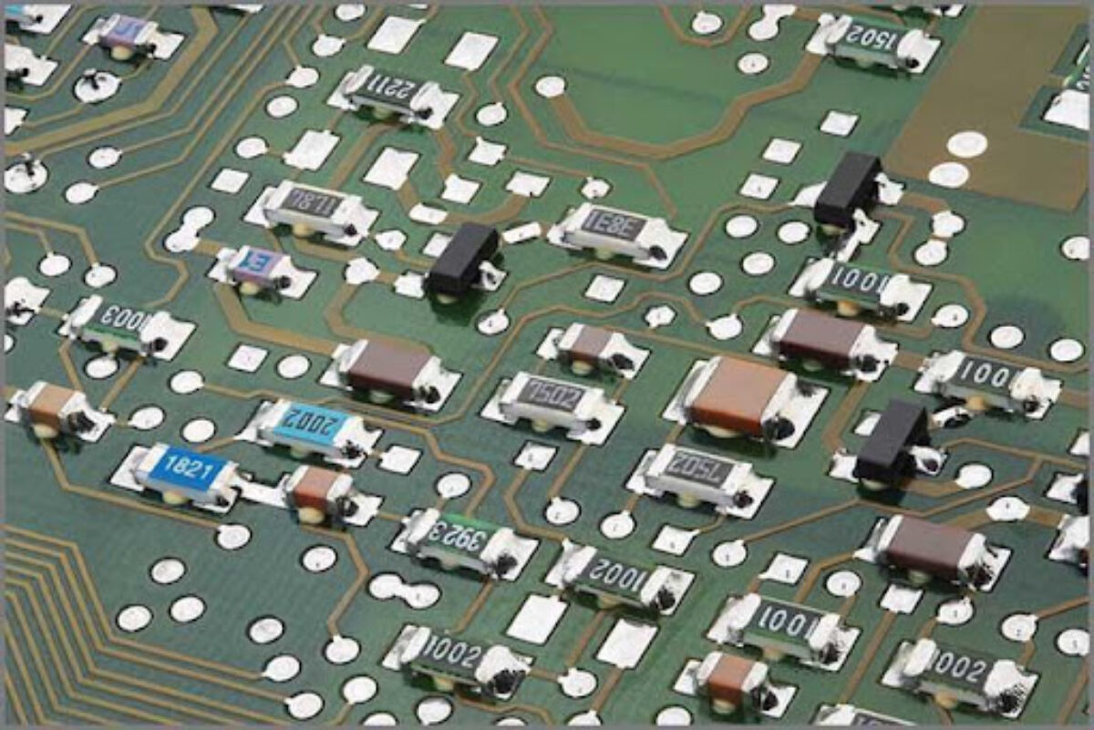
Printed circuit board (PCB) assembly relies heavily on the accurate application of solder paste, especially with surface mount technology (SMT). A meticulously designed stencil acts as the template for this crucial step, directly influencing the final quality of component placement and the integrity of solder joints. Neglecting stencil design can lead to costly manufacturing flaws.
Inadequate stencil design often results in issues like insufficient solder, unintended bridges between pads, or misaligned components. These defects not only compromise the functionality of the board but also necessitate expensive rework and extend production timelines. As electronic devices continue to shrink and component densities increase, the margin for error in stencil design becomes progressively smaller, making precision paramount.
What Are the Fundamental Elements of SMT Stencils?
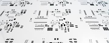
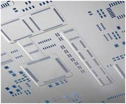
SMT stencils are thin sheets, commonly fabricated from stainless steel, featuring precise laser-cut openings known as apertures. These apertures are carefully aligned with the corresponding pads on a PCB, ensuring that solder paste is deposited exclusively where components will be mounted. Depending on production volume, stencils can be integrated into frames for automated printing or remain frameless for manual operations.
Understanding Stencil Thickness
The typical thickness of a stencil varies, usually ranging from 0.1 mm to 0.2 mm (4 to 8 mils), a choice dictated by the specific type and pitch of components being used. Thinner stencils are generally preferred for fine-pitch components as they deposit a smaller volume of solder paste, minimizing the risk of bridging. Conversely, thicker stencils are better suited for larger components that require more solder paste for robust connections. Striking the right balance is crucial: an overly thin stencil can lead to insufficient solder, while one that is too thick may cause bridging.
Material and Manufacturing Considerations
The material and fabrication process significantly impact a stencil's performance and longevity. Laser-cut stainless steel stencils are favored for their exceptional precision and durability, ensuring consistent results over thousands of print cycles. Some advanced stencils also incorporate nano-coatings, which enhance solder paste release and reduce the frequency of cleaning, contributing to more efficient production.
What Key Factors Influence PCB Assembly Stencil Design?
Crafting an effective stencil for PCB assembly demands careful consideration of several interconnected parameters. Optimizing these factors is essential for achieving superior solder paste deposition and overall board quality.
Aperture Shape and Size
The design of each aperture is central to a stencil's functionality. Its dimensions and form must precisely correspond to the PCB pad, with minor adjustments often made to facilitate proper paste release and meet specific component requirements. For most standard components, apertures are typically designed to be 90-100% of the pad size to prevent excessive paste. However, for fine-pitch components (those with a pitch below 0.5 mm), reducing the aperture to 80-90% of the pad size can significantly mitigate the risk of solder bridging. While rectangular or square apertures are common, designs with rounded corners can improve paste release by eliminating sharp edges where paste might adhere. For Ball Grid Arrays (BGAs), circular apertures are often utilized to complement the spherical solder balls, ensuring uniform deposition.
Optimizing Stencil Thickness and Area Ratio
As previously noted, stencil thickness directly controls the volume of solder paste deposited. A critical guideline is to maintain an area ratio (calculated as the ratio of the aperture opening area to the internal wall area of the aperture) of at least 0.66. This ratio is vital for ensuring proper paste release. For instance, a 0.15 mm thick stencil with a 0.3 mm wide aperture would have an area ratio of 0.5, which is likely to impede smooth paste transfer. Adjusting the stencil thickness or slightly widening the aperture can help achieve a more favorable area ratio and improve deposition.
The Role of Alignment and Fiducial Marks
Precise alignment between the stencil and the PCB is absolutely essential. Fiducial marks—small, distinctive reference points placed on both the PCB and the stencil—assist automated printing machines in achieving perfect registration. It is imperative that these marks are incorporated into the stencil design at locations identical to those on the PCB layout to prevent misalignment during the printing process.
Material Choice for Durability
Stainless steel remains the preferred material for most stencils due to its inherent strength and resistance to wear. For high-volume production, investing in a premium stencil featuring a polished finish or a nano-coating can extend its operational lifespan and enhance paste release, leading to fewer defects and reduced maintenance requirements.
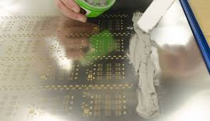
What Techniques Enhance Stencil Printing in SMT Assembly?
Once the stencil is designed, the printing stage becomes the next critical phase. This process involves using a squeegee to push solder paste through the stencil's apertures onto the PCB. Employing specific techniques and adhering to best practices can ensure consistent and high-quality results.
● Squeegee Angle and Pressure: The angle of the squeegee, typically set between 45-60 degrees, significantly influences how uniformly solder paste fills the apertures. A steeper angle might cause the paste to "skip" over smaller apertures, while an angle that is too shallow could lead to excessive paste buildup. Moderate pressure is ideal—sufficient to force paste through the openings without damaging the stencil or the PCB.
● Controlling Print Speed: A slow and steady print speed, usually ranging from 20-40 mm per second, allows the solder paste adequate time to settle correctly into the apertures. Faster speeds can result in incomplete filling, particularly for fine-pitch components, potentially leading to insufficient solder joints.
● Selecting the Right Solder Paste: The choice of solder paste must align with the stencil design, especially regarding particle size. For fine-pitch applications, Type 4 or Type 5 solder paste (with particle sizes of 20-38 microns or 15-25 microns, respectively) is recommended to ensure smooth flow through smaller apertures. Using larger particle sizes risks clogging the openings, leading to inconsistent deposition.
● Regular Cleaning and Maintenance: Consistent cleaning of the stencil is crucial to prevent paste accumulation, which can block apertures and cause defects. Using a lint-free cloth and an appropriate solvent, stencils should be cleaned after every 5-10 prints, or more frequently for high-density designs. Automated printing systems often integrate under-stencil wiping features to streamline this essential maintenance task.
How Can Aperture Design Be Optimized for Maximum Precision?
Aperture design often presents the most significant challenge in stencil creation, particularly for complex boards featuring a variety of component types. Advanced strategies can refine aperture layouts for superior solder paste deposition.
Area Ratio and Aspect Ratio Guidelines
Beyond the area ratio of 0.66, the aspect ratio (the aperture's width relative to the stencil's thickness) should ideally be at least 1.5. For example, a 0.2 mm thick stencil should have apertures no narrower than 0.3 mm to prevent solder paste from sticking to the aperture walls. Adhering to these ratios is fundamental for consistent paste release.
Implementing Step Stencils for Mixed Component Boards
For PCBs that incorporate both fine-pitch and larger components, a step stencil can be a highly effective solution. This stencil features varying thicknesses across different regions: thinner sections for delicate, fine-pitch components and thicker sections for larger ones. This innovative approach helps to balance the volume of solder paste across the entire board, thereby minimizing the likelihood of defects arising from disparate paste requirements.
Specific Considerations for BGAs and QFNs
When dealing with Ball Grid Arrays (BGAs), it's advisable to reduce the aperture size by 10-20% relative to the corresponding pad. This reduction helps prevent excess paste, which could cause solder balls to merge and create shorts. For Quad Flat No-Lead (QFN) packages, a cross-shaped or segmented aperture design is often beneficial. This design helps manage paste volume effectively and mitigates the formation of voids beneath the component, ensuring robust electrical and thermal connections.
What Are Common Stencil Design Hurdles and Their Solutions?
Despite meticulous planning, challenges can arise in stencil design. Understanding common issues and their resolutions can help maintain a smooth PCB assembly process.
● Solder Bridging: This occurs when excessive solder paste connects adjacent pads, often due to oversized apertures or an overly thick stencil. To address bridging, consider reducing aperture sizes by 10-15% or utilizing a thinner stencil specifically for fine-pitch areas. Fine-tuning print pressure and speed can also contribute to a solution.
● Insufficient Solder Paste: If too little solder paste is deposited, components may not adhere correctly during the reflow process. This issue frequently stems from poor solder paste release, often caused by apertures that are too small or an inadequate area ratio. Re-evaluating the area ratio and potentially increasing aperture size or employing a thinner stencil can rectify this.
● Misalignment: Stencil misalignment results in solder paste being applied off-target, leading to incorrect component placement. Thoroughly check fiducial marks and ensure the printing equipment is accurately calibrated. For manual printing, using alignment pins or guides can help secure the stencil properly.
What Are the Best Practices for Effective PCB Assembly Stencil Design?
To consistently achieve high-quality results with SMT stencils, integrating several key best practices is invaluable.
● Collaborate with Manufacturers: Engage closely with your stencil supplier to ensure the design perfectly aligns with your PCB layout and assembly needs. Providing comprehensive Gerber files and detailed specifications will guarantee accurate production.
● Test and Iterate: Before committing to full production, run a small batch of boards to thoroughly test solder paste deposition and component placement. Adjusting aperture sizes or stencil thickness as necessary based on these initial tests is a crucial step.
● Adhere to Industry Standards: Remain current with industry guidelines, such as those established by the Institute for Printed Circuits (IPC). This ensures your stencil designs consistently meet established quality and performance benchmarks.
● Invest in Quality: Opt for superior materials and manufacturing processes, even if the initial investment is higher. Durable and precise stencils reduce defects and the need for rework, ultimately saving both time and financial resources in the long run. As noted by AIVON's engineering team, quality in stencil design is paramount for long-term production efficiency.
Concluding Thoughts: Mastering Stencil Design for Optimal PCB Assembly
Expert stencil design is undeniably a cornerstone of successful PCB assembly, particularly within the precision-demanding SMT process. By meticulously addressing aperture design, selecting appropriate stencil thickness, and refining printing techniques, manufacturers can dramatically enhance the quality of solder paste application and minimize assembly defects. Whether tackling complex, high-density boards or designs with a mix of component types, the insights and strategies presented in this guide offer a robust framework for creating highly efficient SMT stencils.
Remember, effective stencil design synthesizes both scientific principles and practical artistry. It requires careful calculations, thorough testing, and collaborative efforts to achieve optimal outcomes. Embracing the right approach will streamline the PCB assembly process, ensuring the consistent production of reliable, high-performance circuit boards. Apply these principles to your upcoming projects and experience the tangible difference a well-engineered stencil can make.