Why is USB-C a Critical Consideration for Modern PCB Design?
The USB-C connector has rapidly become a cornerstone of modern electronics, redefining how devices connect and exchange data and power. Its compact, reversible design eliminates user frustration, while its multi-functional capability—supporting high-speed data, significant power delivery, and alternative modes like video output—makes it indispensable across various applications, from consumer gadgets to industrial systems. For PCB designers, understanding USB-C's intricacies is crucial for successful product development.
Integrating USB-C effectively requires meticulous attention to detail. A poorly implemented design can lead to a cascade of issues, including degraded signal quality, unstable power delivery, and potential device malfunctions. Conversely, a well-executed USB-C integration ensures robust performance, reliability, and future-proof compatibility. This guide focuses on practical design guidelines to help engineers navigate the complexities of USB-C PCB integration.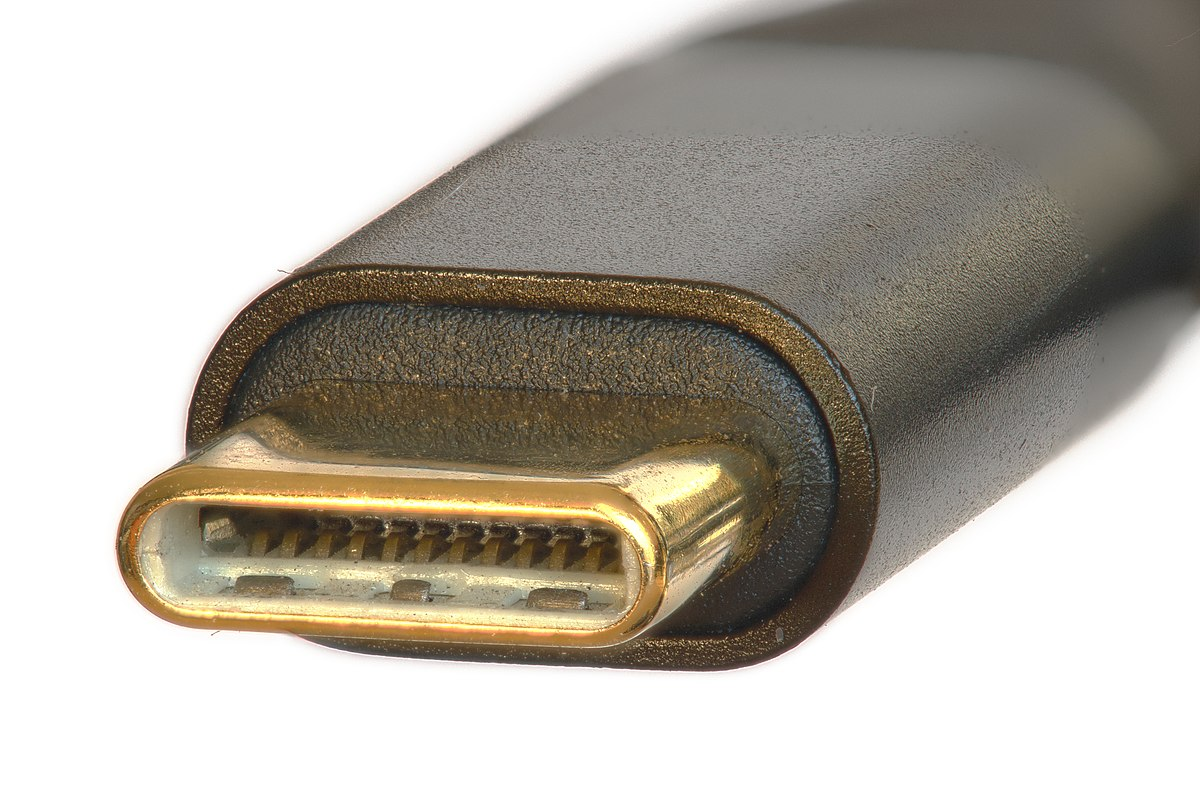
What Key Design Factors Ensure USB-C Reliability?
Achieving a reliable USB-C implementation on a PCB involves addressing several critical design areas. These include maintaining signal integrity for high-speed data, managing power delivery efficiently and safely, and mitigating electromagnetic interference (EMI).
Maintaining Signal Integrity for High-Speed Data
USB-C supports impressive data rates, with USB 2.0 operating at 480 Mbps and USB 3.1 SuperSpeed pairs reaching up to 10 Gbps. To ensure these signals transmit cleanly without errors:
● Controlled Impedance: Route differential pairs to a specific impedance. USB 3.1 typically requires 90 ohms (±10%), while USB 2.0 targets 85 ohms. This is often achieved using a multi-layer PCB with a stable ground plane underneath the traces.
● Length Matching: Keep the traces within each differential pair extremely close in length (e.g., within 5 mils or 0.127 mm). This prevents timing skew, which is particularly vital for USB 3.1's fast signal rise times.
● Minimize Discontinuities: Avoid using excessive vias (through-hole connections) and sharp 90-degree turns in differential pair routing, as these can cause signal reflections. Opt for smooth 45-degree bends instead.
H3: Efficient Power Delivery for High Wattage
USB-C Power Delivery (USB PD) can supply up to 100W (20V at 5A), a significant increase from older USB standards. This capability demands a robust power management design:
● Wide VBUS and GND Traces: Use generously wide traces for the VBUS (power) and GND lines to safely handle high currents without excessive voltage drop or heat buildup. For example, a 5A current may require traces of 50 mils or more on a standard copper layer.
● Decoupling Capacitors: Place both small (e.g., 0.1 µF) and larger (e.g., 10 µF) decoupling capacitors close to the VBUS pins. These help filter noise and maintain stable voltage levels, positioned within 100 mils of the connector.
● CC Pin Configuration: The Configuration Channel (CC1 and CC2) pins are crucial for negotiating power roles. For a device acting as a power sink (drawing power), connect 5.1 kΩ pull-down resistors to ground on both CC lines to signal its capability (e.g., 5V/3A).
Mitigating EMI for Compliance and Performance
High-speed signals and power switching within a USB-C circuit can generate electromagnetic interference (EMI), potentially disrupting other components or failing regulatory compliance. Effective mitigation strategies include:
● Continuous Ground Planes: Ensure USB-C signal traces are routed over unbroken ground planes. Avoid routing over splits or cutouts in the ground plane, which can create undesirable return paths and increase EMI.
● Shielding Connections: Connect the USB-C connector's metal shell to the ground plane using multiple vias (at least four) distributed around the footprint. This provides an effective shield to shunt noise.
● Strategic Component Placement: Maintain adequate separation (e.g., 50 mils) between USB traces and noisy components like high-speed clocks, oscillators, or inductors to prevent signal coupling.
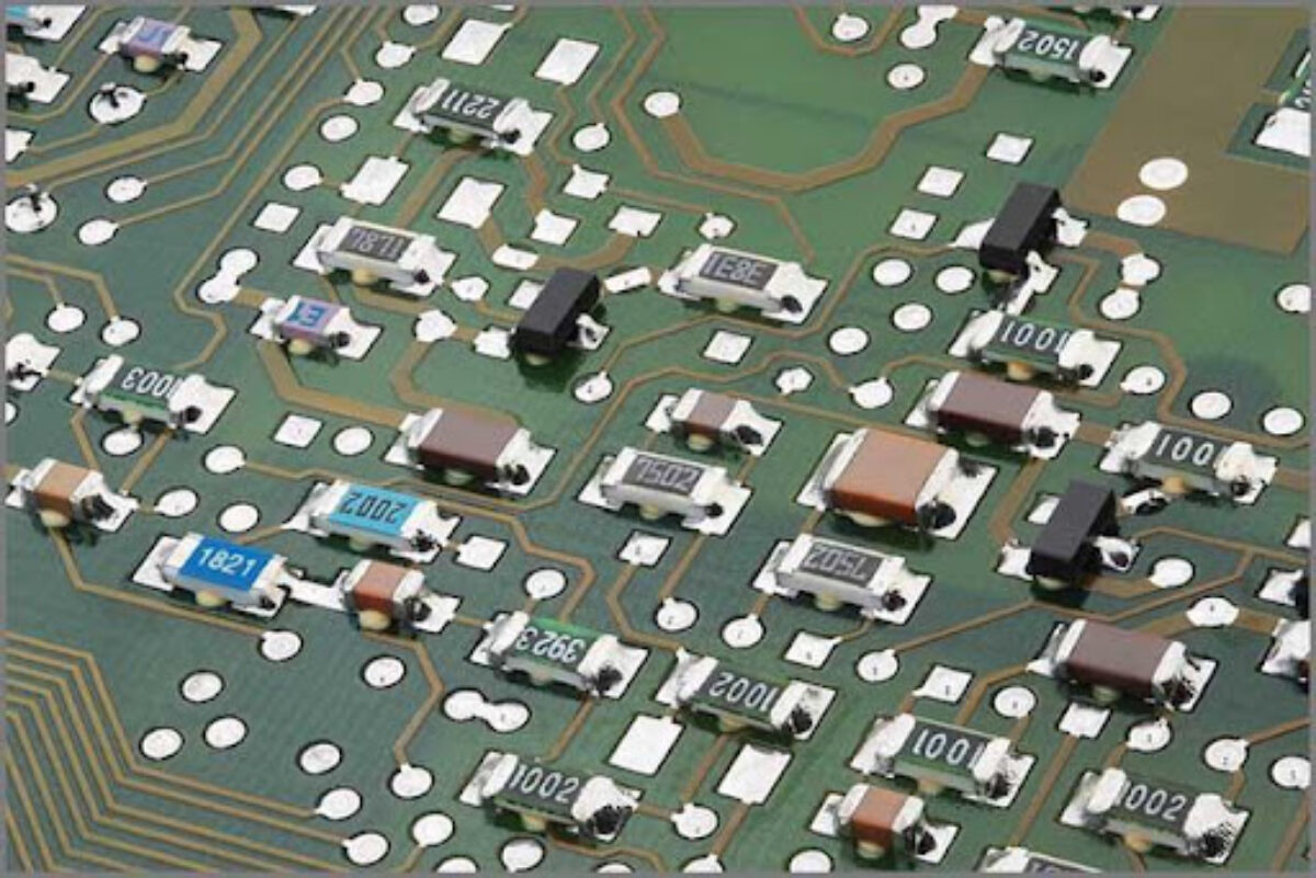
H2: Best Practices for USB-C PCB Layout
Optimal physical layout on the PCB is paramount for realizing the full potential of USB-C. Careful placement and routing minimize signal degradation and enhance overall system stability.
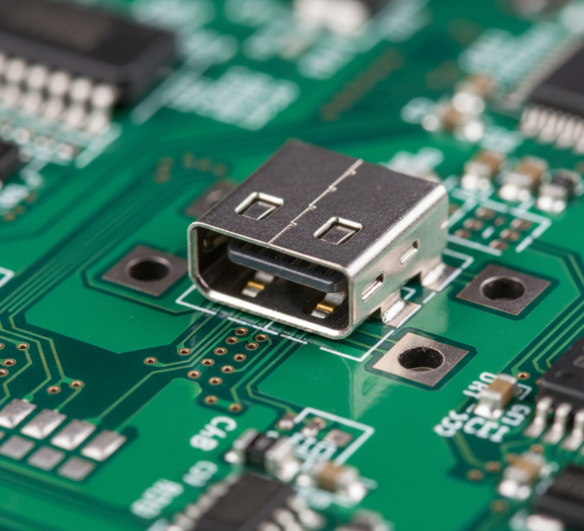
Connector Placement and Mechanical Stability
The USB-C connector should be placed near the edge of the PCB to facilitate easy user access and minimize the length of high-speed traces. For surface-mount connectors, ensure precise alignment with the manufacturer's footprint specifications, typically involving a 0.5mm pin pitch. Integrating through-hole mounting tabs is advisable for enhanced mechanical stability, especially in applications where the connector will experience frequent insertion and removal cycles.
Routing High-Speed Differential Pairs
Both USB 2.0 (D+/D-) and USB 3.1 (TX/RX) differential pairs require careful routing as tightly coupled pairs:
● Maintain a consistent spacing (e.g., 5-8 mils) within each pair and keep them well separated (e.g., at least 20 mils) from other unrelated signals to prevent crosstalk.
● Avoid routing these critical traces underneath noisy components such as crystals, large integrated circuits, or power regulators.
● Utilize length tuning techniques, like serpentine traces, to ensure the lengths of traces within a pair are matched precisely, keeping skew below 5 mils.
Grounding Strategy and Layer Stackup
A 4-layer PCB stackup is highly recommended for USB-C designs, offering a robust foundation for signal integrity and power delivery:
● Layer 1 (Top): Dedicated for critical signal traces and component placement.
● Layer 2: A solid, continuous ground plane serving as a low-inductance return path for high-speed signals.
● Layer 3: Can be used for power distribution or as an additional ground plane, depending on design complexity.
● Layer 4 (Bottom): Suitable for lower-speed signals or secondary routing.
For USB 3.1 SuperSpeed pairs, routing them on the top layer directly over the Layer 2 ground plane minimizes impedance discontinuities. Additionally, incorporating stitching vias along the edges of these traces every 100-200 mils helps connect the ground planes across different layers, further improving EMI performance.
Common Pitfalls and Validation Strategies
Even with careful design, specific challenges can arise during USB-C integration. Awareness of these common issues and employing thorough validation techniques are essential for a successful product.
Avoiding Impedance Mismatches
An impedance mismatch, such as routing 100-ohm traces when 90 ohms is required, can lead to signal reflections and severely degrade data transmission rates. Always use a PCB design tool with an integrated impedance calculator and cross-reference the calculations with your fabricator's specified layer stackup data. Prototyping and testing with a time-domain reflectometer (TDR) can confirm actual impedance values.
Preventing Overheating of Power Traces
Undersized VBUS traces for high currents can cause excessive heat generation, potentially leading to board delamination or outright failure. Consult IPC-2221 standards to calculate appropriate trace widths; for example, a 1 oz copper trace carrying 5A might need to be at least 47 mils wide to keep the temperature rise below 20°C. Thermal simulations are recommended when pushing current limits.
Ensuring Robust ESD Protection
USB-C ports are directly exposed to electrostatic discharge (ESD) events, which can damage sensitive internal circuitry if not adequately protected. Integrate ESD suppressors, such as TVS diodes, rated appropriately for the VBUS voltage (e.g., 5V or 20V). Position these protection components as close as possible (within 50 mils) to the connector pins to be effective.
Comprehensive Design Validation
Before committing to mass production, thorough testing and validation of your USB-C design are critical:
● Signal Integrity Testing: Use a high-speed oscilloscope to examine eye diagrams for both USB 2.0 and USB 3.1 signals. A clear, open eye diagram (e.g., >80% height, <20% jitter) indicates good signal quality and compliance.
● Power Delivery Testing: Conduct load tests on the VBUS line at maximum intended current (e.g., 3A or 5A). Measure the voltage drop to ensure it remains within the specified tolerance (e.g., typically within 5% of the nominal voltage).
● Compliance Certification: For commercial products, pursue USB-IF certification. Specialized tools, such as the Ellisys USB Explorer, can automate these rigorous compliance tests.
Prototyping and iterative testing are invaluable, helping to identify and resolve potential issues early in the development cycle, thereby saving significant time and cost.
Partnering for USB-C Design Success
For engineers navigating the complexities of USB-C integration, collaborating with an experienced PCB manufacturer can be a significant advantage. AIVON offers rapid PCB prototyping services, enabling quick iteration and testing of designs to fine-tune signal routing and power networks efficiently. Their advanced manufacturing capabilities are well-suited for the tight tolerances required by USB-C, such as 6-mil traces and 0.5mm-pitch footprints. With efficient global logistics, AIVON supports project timelines wherever development takes place. This partnership helps transform USB-C design concepts into reliable, high-performing reality.