Introduction
In the early 19th century Sharp and the Japanese telecommunications operator J-PHONE developed the Sharp J-SH04, which had a camera function. On April 24, 2003 Sharp released the world's first one-megapixel mobile phone, the J-SH53.
With continuous technological advances, new camera modules have emerged steadily, moving from early one-megapixel designs to tens of megapixels over more than a decade. Companies such as Huawei, Samsung, and Apple have advanced lens and image-processing chip designs. Concepts that were theoretical years ago, such as dual-camera systems, are now implemented in commercially available phones.
Most phones on the market have both front and rear cameras. Front cameras are typically around 5 MP for selfies and video calls. Rear cameras are commonly around 13 MP and produce higher-resolution photos and clearer video recordings.
Mobile Camera Components
Mobile camera modules mainly consist of: PCB, DSP (used in CCD systems), image sensor (SENSOR), holder, and lens assembly (LENS ASS'Y). The three most important components are the lens assembly, the DSP (for CCD-based modules), and the sensor.
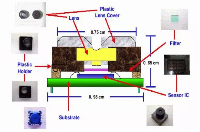
PCB
PCB types include rigid, flexible, and rigid-flex boards. CMOS sensors can use any of these board types, while CCD sensors typically require rigid-flex boards. Rigid-flex boards are usually the most expensive, and rigid boards the least expensive.
Lens
The lens is the second most important factor affecting image quality after the sensor. A lens is composed of multiple lens elements and is generally classified as plastic (resin) lens or glass lens. Resin lenses are not pure plastic but are molded resin elements; their optical properties such as transmittance and sensitivity are inferior to coated glass elements.
Common lens constructions for camera modules include: 1P, 2P, 1G1P, 1G2P, 2G2P, 2G3P, 4G, 5G, and so on. More lens elements generally increase cost and improve imaging performance. Glass elements are more expensive than resin. A high-quality camera module typically uses multiple glass elements, while many low-cost modules use resin or mixed glass-resin designs, which negatively affect imaging performance.
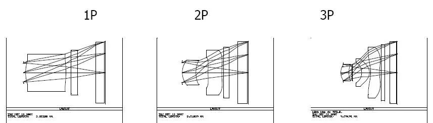
The lens assembly consists of lens elements, optical filters, and the barrel. Three primary optical parameters are focal length f', relative aperture D/f', and field of view 2ω.
Focal length is an important parameter that determines the size relationship between object and image. For an object at infinity, the image size is given by y' = -f' * tan ω, where ω is the object-side field angle.
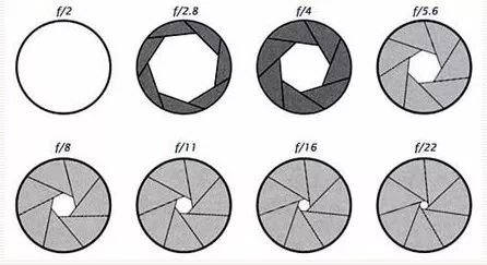
Relative aperture D/f' and the f-number are key optical indicators. Relative aperture denotes the proportion of light entering the lens that reaches the image plane. It is defined as the entrance pupil diameter D divided by the focal length f'. Low-light and fast-motion photography require a large relative aperture to increase image-plane illumination. Lenses are classified by relative aperture into weak-light lenses (D/f' 1:6.3 and smaller), ordinary lenses (D/f' 1:3.5), strong-light lenses (D/f' 1:2.8–1:1.4), and ultra-strong-light lenses (D/f' 1:1–1:0.8). Apertures are typically adjustable, allowing adaptation to different shooting environments.
The reciprocal of the relative aperture is the f-number, commonly labeled on camera lenses. Standard f-numbers include 0.7, 1, 1.4, 2, 2.8, 4, 5.6, 8, 11, 16, 22, ... As the f-number increases, the aperture becomes smaller and transmitted light is reduced by half for each full stop. For photography, lower f-numbers provide greater lens compatibility and versatility. Relative aperture also affects depth of field; changing the aperture controls depth of field during shooting.
The field of view 2ω determines the angular extent of the scene the lens captures. The usable field is defined by the diameter of the circular region on the image plane that delivers acceptable image quality, or by the size of the imaging surface of the chosen image sensor.
Basic lens types include: by focal length and field of view—standard, wide-angle, and telephoto lenses; by whether focal length is variable—fixed focal (prime) and zoom lenses.
Holder and Color Filter
The holder secures the lens assembly. A color filter element is often placed on or near the holder.
Two common color filter arrays are the RGB primary-color filter and the CMYK complementary-color filter. Primary-color CCDs offer sharp image quality and realistic color but tend to be noisier; cameras using a primary-color CCD typically limit ISO sensitivity to around 400. Complementary-color CCDs include a yellow (Y) filter, sacrificing some resolution but allowing higher ISO settings, often above ISO 800.
DSP (Digital Signal Processing Chip)
The DSP performs complex mathematical algorithms to optimize digital image signals and outputs the processed signal to display or storage.
Typical DSP architecture includes: (1) ISP (image signal processor) and (2) JPEG encoder. ISP performance is critical for smooth image processing; JPEG encoder performance is also a key metric. JPEG encoding may be performed by hardware-based JPEG encoders or by software RGB compression.
The DSP or control chip transfers the data captured by the image sensor promptly to the baseband and refreshes the sensor. The quality of this control chip directly affects image attributes such as color saturation, sharpness, and throughput.
In CCD-based camera modules, DSP is a separate component. In CMOS-based modules, DSP functions are often integrated into the CMOS sensor, appearing as a single integrated unit.
Image Sensor
The image sensor is the most important component of a camera module because the photosensitive device largely determines imaging quality.
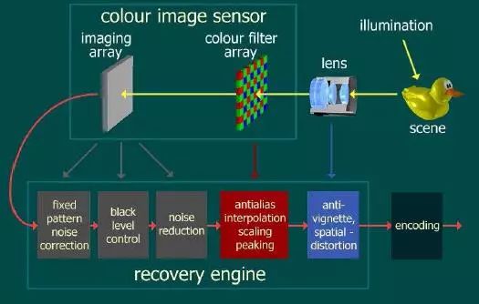
The sensor converts incident light from the lens into electrical signals, which are then converted internally to digital signals via on-chip A/D conversion. Each pixel on a sensor is sensitive to only one color component—R, G, or B—so pixel values are initially monochrome; this raw data is known as RAW data. An ISP is required to reconstruct full-color images from RAW data.
Image sensors function like photographic film. Two main types are CMOS and CCD. CCDs, also called charge-coupled devices, form either one-dimensional linear sensors or two-dimensional area image sensors from arrays of photodiodes.
CCD sensors consist of photodiode light-detecting elements, charge-transfer components, and charge-amplifying circuitry. Photons generate charges that accumulate; with applied gate voltages, accumulated charges are transferred and amplified, producing output charge signals containing image information.
Sensors have trended toward higher sensitivity, higher resolution, lower power consumption, and low-voltage operation.
CMOS image sensors are built from metal-oxide semiconductor technology. Each pixel can integrate multiple devices such as amplifiers and A/D converters.
Differences between CCD and CMOS: CCDs historically produced higher image quality but are complex to manufacture and consume more power. CMOS sensors are simpler, lower-power, and can integrate additional circuitry at the pixel level, enabling per-pixel amplification and processing. These characteristics historically led to higher noise in CMOS designs. If CMOS noise performance improves, CMOS could surpass CCD as the preferred image sensor type.
Some suppliers promote back-illuminated or BSI sensors. BSI is an architecture for CMOS sensors that improves light collection efficiency compared with traditional front-illuminated CMOS, yielding better low-light performance.
Stacked sensor architectures were later introduced. Stacked sensors are not an evolution of BSI per se but a parallel architecture. Stacked sensors enable either smaller sensor sizes for a given pixel count or higher pixel densities in the same footprint, allowing thinner, lighter device designs.
Imaging Principle of Mobile Cameras
Object-side light enters the optical system and passes through the lens to the image sensor. Photons generate mobile charges in the sensor via the internal photoelectric effect. The accumulated charges form electrical signals, which must be converted to digital signals for further processing. In CMOS-based sensor systems, on-chip A/D conversion is often present, so external A/D converters may not be required. In CCD-based systems, an external A/D converter is typically used to convert charge signals into digital data. Digital signals are amplified, processed by a microprocessor and DSP, stored, and finally rendered on a display as an image resembling the original scene.
Key Factors Affecting Mobile Camera Performance
Pixels
The stated "X megapixels" refers to sensor resolution, determined by the number of pixels (the smallest photosensitive units) on the sensor. For example, 5 MP means 5 million pixels. This is analogous to display resolution such as 720p or 1080p.
Do pixels determine image quality? Pixel count only determines the resolution or image size. A higher-resolution image is larger, but not necessarily clearer.
Most current mainstream phone displays are 1080p (1920×1080). Photos from a 13 MP sensor (4208×3120) or an 8 MP sensor (3200×2400) exceed 1080p display resolution, so both will typically be downscaled to 1920×1080 for display, making perceived sharpness similar on the device screen.
Where higher pixel counts are advantageous is in print size. At a standard 300 pixels per inch printing density, a 13 MP image at 4208×3120 can be printed up to approximately 17 inches, while an 8 MP image at 3200×2400 begins to blur beyond roughly 13 inches. Thus, higher-resolution sensors produce larger printable images.
Sensor
If pixels do not solely determine image quality, the sensor is the decisive factor. Two main sensor types are CCD and CMOS. CCDs can deliver excellent image quality but are expensive and less common in phones. CMOS sensors are widely used in mobile devices due to lower power consumption, lower cost, and good image performance.
CMOS sensors include back-illuminated (BSI) and stacked architectures. These technologies were initially developed by Sony, with product names such as Exmor R for BSI and Exmor RS for stacked sensors.
Larger sensors capture more photons, improving signal-to-noise ratio and image quality, but larger sensors increase device size, weight, and cost. BSI sensors improve light collection efficiency in the same sensor footprint, effectively enhancing low-light performance.
Stacked sensors allow smaller sensor sizes for a given pixel count or enable higher pixel densities while saving space, which helps make phones thinner and lighter.
Lens
The lens focuses the scene onto the sensor and acts as the device's "eye." It typically consists of multiple elements that reduce stray light such as infrared and other unwanted wavelengths. In general, more lens elements yield more accurate imaging.
Aperture
The aperture is formed by several thin blades and controls the amount of light reaching the sensor by changing the aperture diameter. Aperture values are typically written as f/2.2, f/2.4, etc.; smaller numbers indicate larger apertures.
A larger aperture allows more light to reach the sensor, producing brighter images, which is advantageous in low-light conditions. Aperture also controls depth of field; a wider aperture results in shallower depth of field and stronger background blur, emphasizing the subject.