Why Is Solder Paste Stencil Design Crucial for SMT Assembly?
In the intricate process of surface mount technology (SMT) assembly, achieving precise solder paste deposition is paramount for producing high-quality printed circuit boards (PCBs). The stencil acts as a fundamental tool in this stage, ensuring reliable solder joints, reducing manufacturing defects, and enhancing overall production efficiency. The core of this process lies in the design of the stencil apertures—a careful balance involving material choice, stencil thickness, and the specific dimensions and shapes of the openings. These elements directly influence how solder paste is applied.
Understanding how to customize aperture designs to meet your PCB's unique specifications can be a decisive factor in the success of your assembly outcomes, whether you are creating prototypes or scaling up for mass production. This guide delves into the vital considerations for achieving optimal solder paste deposition and avoiding common production issues.
What Key Factors Influence Solder Paste Stencil Aperture Design?
The effectiveness of solder paste application hinges on several critical design elements. Each factor plays a significant role in determining the volume, shape, and precise placement of solder paste on PCB pads.
Stencil Thickness and Paste Volume
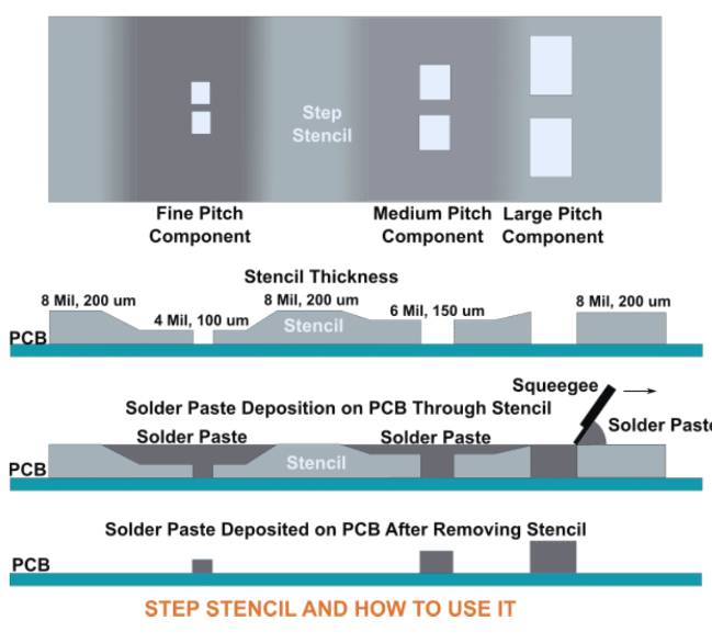
The thickness of a stencil directly governs the amount of solder paste deposited. A thicker stencil delivers more paste, which is generally suitable for larger components like 1206 resistors or various connectors. Conversely, thinner stencils are ideal for fine-pitch components, such as 0201 chip components or Ball Grid Arrays (BGAs), where excess paste can lead to bridging. Stencil thicknesses commonly range from 0.08 mm to 0.15 mm, with 0.12 mm being a frequent choice for many applications. For instance, a 0.10 mm stencil might be preferred for 0201 components to prevent bridging, while a 0.15 mm stencil would be selected for larger parts requiring a greater solder volume. For boards featuring a mix of component sizes, stepped stencils—which have areas of varying thickness—can be utilized to provide tailored paste volumes, although this can introduce challenges with even squeegee pressure.
Aperture Size and Shape
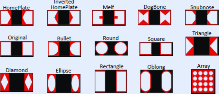
The dimensions of an aperture directly impact the quantity of solder paste transferred to the PCB. As a general guideline, apertures should be slightly smaller than their corresponding PCB pads, typically by about 10%, to prevent solder paste from spreading and causing bridging. For example, with fine-pitch components like 0.4 mm pitch QFPs, the aperture width might need to be reduced to 85% of the pad size, while the length could be extended to 110% to ensure sufficient paste coverage. Beyond size, the shape of the aperture also matters. Standard shapes include rectangles and circles, but specialized forms like home-plate or inverse home-plate designs are used for small chip components (e.g., 0402) to better manage paste volume and reduce solder bead formation. For BGAs, circular apertures are often reduced by 0.05 mm compared to pad size for pitches exceeding 1.0 mm, while ceramic BGAs might require slightly larger apertures (0.05-0.08 mm) to accommodate thermal expansion differences.
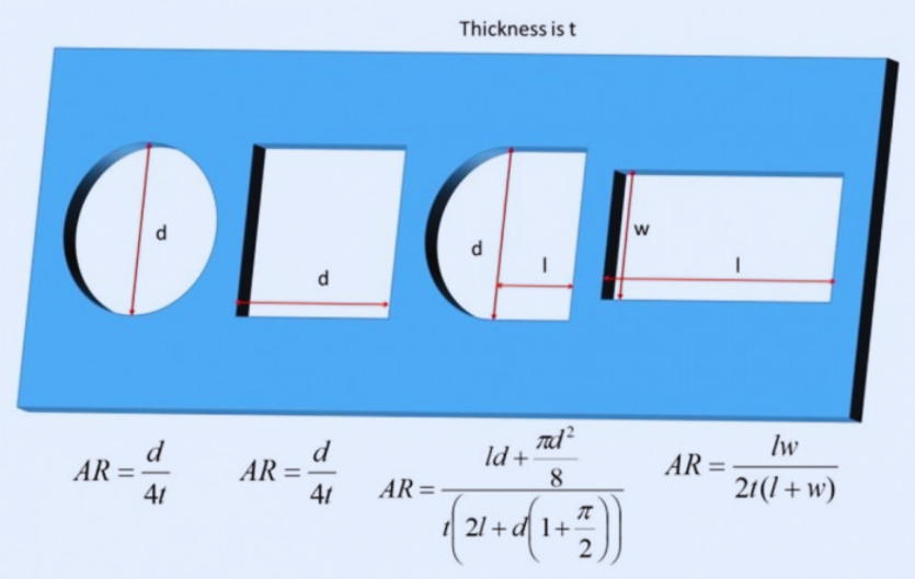
Aspect and Area Ratios for Paste Release
Effective solder paste release depends on two critical ratios: the aspect ratio and the area ratio. The aspect ratio, calculated as the aperture width divided by the stencil thickness (W/T), should ideally be at least 1.5. The area ratio, determined by dividing the aperture area by the total surface area of its walls ((L × W) / [2 × (L + W) × T]), should be at least 0.66. These ratios are essential for ensuring that solder paste cleanly detaches from the aperture walls and transfers accurately onto the PCB pad, rather than adhering to the stencil due to surface tension. For example, a 0.4 mm wide aperture in a 0.12 mm thick stencil yields an aspect ratio of 3.33, well above the minimum. However, for ultra-fine-pitch components, laser-cut stencils with electropolished walls can achieve aspect ratios as low as 1.1, significantly improving paste transfer efficiency (PTE).
Stencil Material and Manufacturing Techniques
Stencils are commonly produced from stainless steel or nickel, chosen for their precision and durability. Stainless steel is a popular choice due to its robustness and cost-effectiveness, while nickel is preferred for high-density applications because of its smoother aperture walls. Fabrication methods vary:
● Laser Cutting: This method offers high precision and results in trapezoidal aperture walls, which enhance paste release. It's ideal for fine-pitch components and complex designs.
● Chemical Etching: While cost-effective for larger apertures, it lacks the precision needed for fine-pitch applications below 0.5 mm.
● Electroforming: This technique creates ultra-smooth, tapered aperture walls, suitable for high-density boards, though it is a more expensive option typically reserved for high-volume production.
Electropolishing or micro-plating can further refine aperture wall smoothness, improving PTE, which is the ratio of deposited paste volume to the theoretical aperture volume. Optimal results aim for a PTE close to 1. Laser-cut stainless steel stencils with electropolished walls often achieve PTE values of 0.8 or higher, particularly for components like QFNs and BGAs.
Importance of Alignment and Fiducial Marks
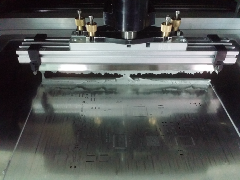
Accurate alignment between the stencil and the PCB is vital for depositing solder paste precisely on the pads. Fiducial marks—small, distinct features present on both the PCB and the stencil—serve as crucial reference points for automated stencil printers. These marks are usually circular or cross-shaped and are included in the PCB's Gerber files. Even slight misalignment, by just a few microns, can lead to paste deposition errors, resulting in defects such as solder bridges or open circuits. For double-sided PCBs, precise alignment becomes even more critical. While a single stencil can be used for both sides, the design must consider component orientation to prevent issues like tombstoning, where components lift during reflow due to uneven heating.
What Are Best Practices for Optimizing Stencil Aperture Design?
To achieve superior results in SMT assembly, engineers should adopt several key practices when designing stencil apertures.
Adhering to Industry Standards and Customization
It's essential to comply with IPC-7525 guidelines for aspect and area ratios to ensure reliable paste transfer. Aperture designs should be customized based on component pitch and type; for example, reducing aperture size by 10-20% for fine-pitch components helps prevent bridging. Additionally, consider the properties of the solder paste itself. Paste viscosity and particle size affect deposition, with finer-grain pastes (e.g., Type 4 or 5) being more suitable for smaller apertures. SAC305 alloys are commonly used for lead-free soldering.
Enhancing Paste Release and Maintenance
Utilizing laser-cut stencils with trapezoidal apertures (wider at the bottom) can significantly improve paste release by minimizing surface tension. Regular cleaning and inspection of stencils are also crucial. Stencils should be cleaned after each use with isopropyl alcohol (IPA) or automated cleaning systems to prevent paste residue buildup, which can clog apertures and degrade print quality. Routine inspection for wear or damage helps maintain printing consistency.
How Can Common Stencil Design Challenges Be Resolved?
Several issues can arise during the solder paste printing process, but targeted design adjustments and practices can mitigate them.
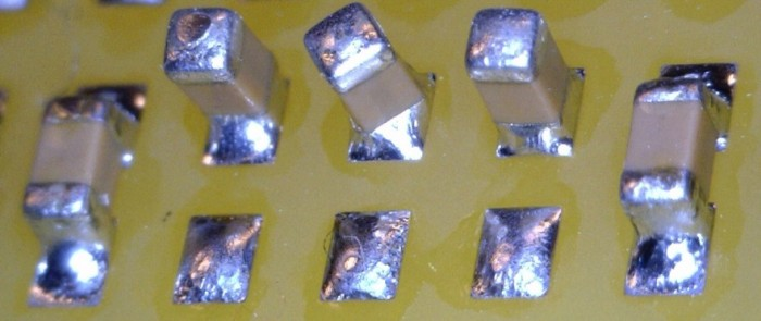
Addressing Solder Bridging
Solder bridging, where excess paste connects adjacent pads, often results from oversized apertures or overly thick stencils. To prevent this, reduce aperture size by 10-20% relative to the pad size and ensure the area ratio exceeds 0.66. For fine-pitch components, consider using electropolished, laser-cut stencils to enhance paste release.
Resolving Insufficient Solder
Insufficient solder paste can lead to weak joints or non-wetting. This issue commonly stems from undersized apertures or poor paste release due to low area ratios. Slightly increasing aperture size or using a thinner stencil can help. For instance, a 0.08 mm stencil might be necessary for 0201 components to ensure adequate paste transfer.
Preventing Tombstoning
Tombstoning, where small components stand upright during reflow, can occur due to uneven paste deposition or misalignment. To counter this, ensure consistent aperture sizes and proper PCB orientation during printing to achieve balanced solder reflow. For double-sided boards, orient components broadside to the direction of travel to facilitate simultaneous soldering of both leads.
Partnering for Optimized SMT Stencil Solutions
For engineers aiming to optimize their SMT assembly processes, collaborating with a reliable manufacturing service provider is crucial. AIVON offers high-precision PCB stencils specifically tailored to meet diverse design requirements, whether for prototyping or large-scale production. Our advanced laser-cutting technology ensures smooth, trapezoidal apertures for superior paste release, while our rapid prototyping services facilitate quick design iterations. With robust global logistics and a steadfast commitment to quality, AIVON supports the achievement of defect-free assemblies, eliminating the complexities of in-house stencil fabrication.
Final Thoughts on Solder Paste Stencil Optimization
The design of solder paste stencil apertures is a vital element in SMT assembly, directly influencing the quality and dependability of PCB solder joints. By meticulously selecting stencil thickness, aperture size and shape, and fabrication methods, engineers can achieve precise solder paste deposition, minimize defects, and enhance manufacturing yields. Adhering to industry standards like IPC-7525, employing advanced fabrication techniques such as laser cutting, and maintaining diligent stencil care are all essential for success in this field.
As PCB designs evolve, incorporating finer pitches and denser layouts, the importance of optimized stencil aperture design will only continue to grow. By adopting these best practices and utilizing high-quality manufacturing services, engineers can ensure their assemblies consistently meet the highest benchmarks for performance and reliability.