What is the Solder Mask Layer in PCB Manufacturing?
Many newcomers to printed circuit board (PCB) design often confuse the solder mask and paste mask layers due to their apparent similarities. However, these two layers serve distinct purposes and are applied at different stages of the PCB fabrication and assembly process. Understanding their individual roles is fundamental for producing reliable and functional circuit boards.
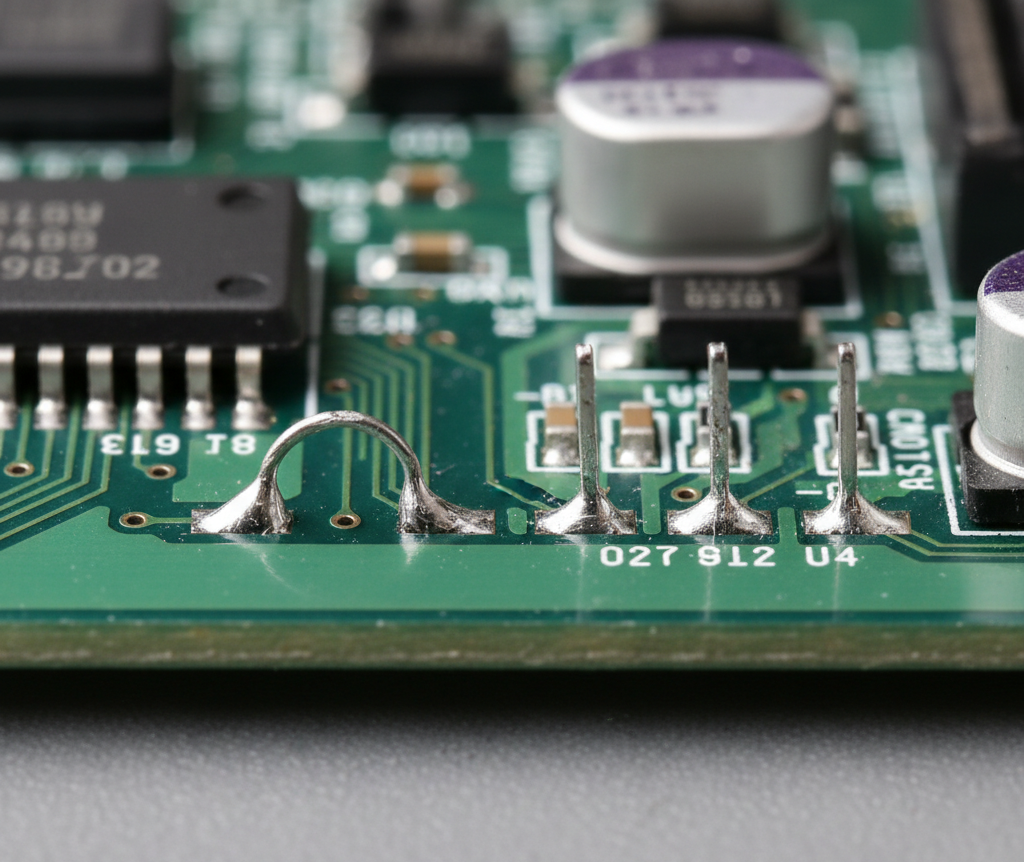
The solder mask is a permanent protective layer applied to a PCB. Its primary function is to cover all areas of the board except for the designated pads (surface mount pads, through-hole pads, and vias). This protective coating, typically an epoxy-based polymer, prevents solder from bridging between adjacent traces or pads during the soldering process, particularly during wave soldering. It effectively insulates the copper traces and helps define specific areas where solder should adhere. This layer is commonly referred to as the "solder resist layer" or simply the "green layer," though it can come in various colors.
Solder Mask Top and Bottom Layers
In Gerber files, which are the standard output for PCB manufacturing, the solder mask is typically divided into "Top Solder Mask" and "Bottom Solder Mask" layers. These layers define the openings (often represented as small circles or squares) where the copper pads are to remain exposed. The openings in the solder mask are generally slightly larger than the pads themselves to ensure the entire pad surface is available for soldering. This slight enlargement is known as solder mask clearance and is crucial for proper solder joint formation.
What is the Paste Mask Layer in PCB Assembly?
In contrast to the solder mask, the paste mask layer is directly related to the surface mount technology (SMT) assembly process and is not an integral part of the PCB itself. It dictates where solder paste will be applied to the board.
Understanding the PCB Stencil
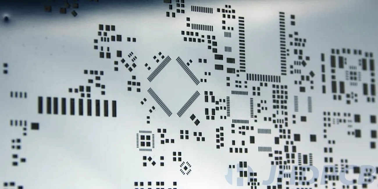
The paste mask layer is essentially the design for a PCB stencil, which is a thin metal sheet with precisely cut-out openings. These openings correspond directly to the SMD (Surface Mount Device) pads on the PCB where components will be soldered. The size of these openings is typically the same as the SMD pads or slightly smaller, a practice known as "paste mask reduction." This stencil is indispensable in the automated SMD assembly process for accurately applying solder paste onto the pads.
During assembly, the stencil is precisely aligned over the circuit board. Solder paste—a mixture of tiny solder spheres and flux—is then spread across the stencil. A squeegee blade removes any excess paste, ensuring that solder paste is deposited only through the stencil's apertures onto the designated pads. Once the stencil is removed, components are placed onto these solder paste deposits (either manually or by an assembly machine), and the entire assembly then passes through a reflow oven to melt the solder paste and form the electrical connections. The paste mask layer is also divided into "Top Paste" and "Bottom Paste" for boards with components on both sides.
Key Differences Between Solder Mask and Paste Mask
While both layers involve "mask" and relate to soldering, their functions, physical properties, and application stages are fundamentally different.
Functional and Physical Distinctions
● Presence of Material: Openings on the solder mask layer mean there is no solder mask ink present, leaving copper exposed. Conversely, openings on the paste mask layer indicate where solder paste will be deposited.
● Part of the PCB: The solder mask is an integral, permanent layer of the finished circuit board, providing insulation and protection. The paste mask, however, is a design file used to create a separate physical tool (the stencil) and is not part of the final PCB itself.
● Purpose of Application: The solder mask is applied to insulate and prevent unwanted solder bridges. The paste mask is used to precisely apply solder paste onto component pads for attachment.
● Timing of Application: The solder mask is applied during the actual PCB manufacturing process (fabrication). The paste mask (stencil) is used during the later component assembly stage.
● Coloration: Solder masks come in various colors (green, blue, red, black, etc.). Paste masks, being stencil designs, are typically represented as grey or a neutral color in design software.
Practical Tips for Beginners: Avoiding Common Mask Mistakes
Beginners in PCB design frequently encounter issues with mask layers, leading to significant problems during assembly. Careful attention to these details can prevent costly rework.
Common Errors and Solutions
When designing pads in PCB software, it's easy to overlook crucial mask layer settings. Forgetting to create an opening in the solder mask for a pad, or misaligning paste mask apertures, can result in poor solder joints, "cold" solder connections, or incorrect component placement. To mitigate these risks, AIVON provides complimentary DFM (Design for Manufacturability) checks that meticulously review your Gerber files prior to production. This service ensures that both your solder mask and paste mask layers are correctly configured, which is especially critical for complex designs like 4-layer PCBs with intricate stack-ups and dense pad arrangements.
AIVON also offers guidance on best practices, including:
● Solder Mask Clearance: Maintaining adequate clearance around vias and pads to prevent solder bridging between adjacent features.
● Paste Mask Reduction: Adjusting the size of paste mask apertures based on the component type to ensure the optimal volume of solder paste is deposited.
● Alignment: Ensuring precise alignment of paste mask apertures with component orientation, particularly for fine-pitch integrated circuits (ICs) and Ball Grid Arrays (BGAs).
How Mask Layers Interact with Panelization and Mouse Bites
When moving a PCB design from a single board to a production panel, panelization becomes a key consideration. For smaller or unusually shaped boards, mouse bites are a common depanelization technique, offering an alternative to V-scoring by creating small perforated tabs between boards.
Mask Considerations for Depanelization Zones
It is critical to understand how solder and paste mask layers must be managed in these depanelization areas:
● Solder Mask Near Mouse Bites: Avoid placing components or pads too close to mouse bites. Insufficient solder mask coverage in these areas can lead to exposed copper or unintended solder bridges.
● Paste Mask and Depanelization: Ensure that paste mask apertures do not overlap with any depanelization zones (like mouse bites). Solder paste deposited in these areas could smear during the board separation process, causing shorts or assembly defects.
AIVON’s engineering team specializes in optimizing panel layouts to minimize mechanical stress on PCBs during depaneling, preserve the integrity of pads, and reduce overall custom PCB costs by efficiently minimizing material waste.
AIVON: Your Partner for PCB Success
Whether your project is a straightforward beginner-level circuit or a sophisticated industrial-grade PCB, a clear understanding of the distinctions between solder mask and paste mask is vital for achieving robust and reliable assemblies. From advanced depanelization options like mouse bites and V-cut PCBs to intricate 4-layer PCB fabrication, AIVON consistently delivers high quality, rapid turnaround, and transparent control over your custom PCB costs.
By choosing AIVON, you benefit from:
● Free DFM Checks: Ensuring design manufacturability before production.
● Rapid Prototyping & Mass Production: Flexible options to meet project scale and timeline.
● Reliable Panelization: Expertise in mouse bites and V-cut options for efficient board separation.
● Expert Support: Comprehensive assistance for boards ranging from 2-layer to 32+ layer designs.
● Transparent Pricing: Clear and competitive cost structures for all custom PCB needs.