What is Tombstoning and What Triggers It?
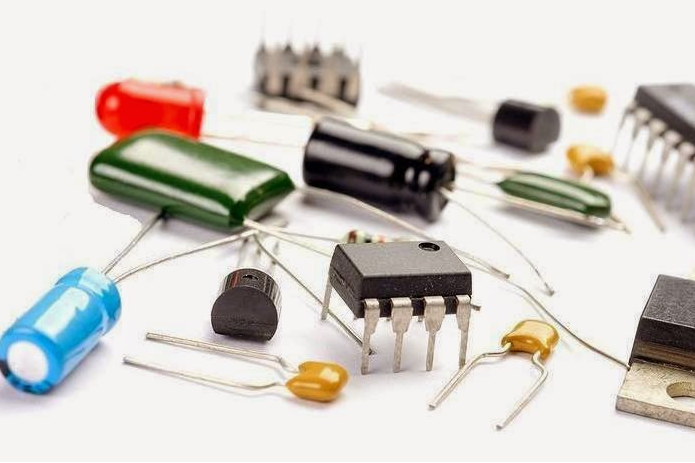
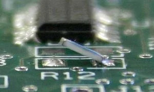
Tombstoning, a frustrating defect in PCB assembly, occurs when a surface-mount device (SMD) component, such as a resistor or capacitor, lifts off one of its pads during the soldering process. This leaves it standing upright, resembling a tombstone—a phenomenon also referred to as the 'Manhattan effect' or 'drawbridge effect.' Predominantly seen in small passive components like 0402 or 0201 package sizes, even minor imbalances can lead to this significant issue, resulting in an open circuit that renders the component—and potentially the entire board—inoperable.
At its core, tombstoning is a consequence of uneven wetting forces during the reflow soldering process. Wetting describes the phenomenon where molten solder paste flows and creates a bond with both the component's termination and the PCB pad. Ideally, the solder on both pads melts and solidifies simultaneously, anchoring the component evenly. However, if one pad achieves wetting before the other, the resulting surface tension pulls the component towards the side where wetting has already occurred, causing it to tilt or "tombstone." Several key factors can precipitate this imbalance:
● Temperature differences: Inconsistencies in oven temperature or variations in thermal mass across the board can cause one pad to heat and melt solder more rapidly.
● Component size: Smaller components, possessing less mass and surface area, are inherently more susceptible to lifting. For example, an 0201 package (0.6 mm x 0.3 mm) is significantly more prone to tombstoning than a larger 0805 package (2.0 mm x 1.25 mm).
● Pad design flaws: Disparities in pad sizes or improper spacing can disrupt uniform heating and wetting. A larger pad, for instance, may require more time to reach the optimal soldering temperature.
● Solder paste issues: An excessive amount of solder paste on one pad or inconsistent application via the stencil can accelerate wetting on one side.
● Surface finish variations: Uneven PCB surface finishes, such as those sometimes found with Hot Air Solder Leveling (HASL), can impede consistent solder flow, thereby increasing the risk of tombstoning.
A thorough understanding of these underlying causes is crucial for preventing tombstoning. By proactively addressing these factors, manufacturers and engineers can ensure that SMD components remain perfectly seated and fully functional.
The Far-Reaching Impact of Tombstoning on PCB Assembly
Tombstoning is far more than a mere aesthetic imperfection; it represents a significant defect that can profoundly disrupt an entire PCB assembly project. Its implications for engineers and manufacturers are substantial:
● Open circuits: A lifted component severs the electrical connection, leading to immediate functional failure. In complex circuits, this can completely halt system operation.
● Increased costs: Reworking boards affected by tombstoning incurs additional labor and material expenses. In high-volume production, even a modest 1% defect rate can translate into thousands of dollars in financial losses.
● Reliability risks: Reworked solder joints may not possess the same mechanical strength or electrical integrity as properly formed joints, potentially leading to long-term reliability issues. For critical applications, such as medical devices or automotive electronics, this level of risk is unacceptable.
● Reduced yields: The presence of tombstoning directly lowers the number of usable boards produced from an assembly line, necessitating extra inspection steps or a slower production pace to identify and rectify defects.
Given the high stakes involved, particularly where precision and operational uptime are critical, preventing tombstoning is not merely about avoiding minor inconveniences. It is fundamentally about upholding quality standards, maximizing production efficiency, and ensuring ultimate customer satisfaction.
Actionable Strategies to Prevent Tombstoning in PCB Assembly
Preventing tombstoning demands a synergistic approach, combining intelligent design choices with meticulous assembly practices. The following section details seven practical strategies that engineers and manufacturers can implement to ensure SMD components remain securely in place. Each tip is supported by actionable steps for immediate application.
Design Optimizations for Pad Layout
1. Optimize Pad Design: Pad design serves as the primary defense against tombstoning. Symmetrical and appropriately sized pads are crucial for promoting uniform solder wetting and heating.
● Adhere to IPC standards: Consult IPC-7351 guidelines for recommended pad dimensions specific to your SMD components. For example, an 0402 resistor might require pads of 0.5 mm x 0.6 mm with a 0.4 mm gap.
● Ensure matching pad sizes: Discrepancies in pad size (e.g., one pad being 20% larger) will cause uneven heating and delayed wetting. Maintain identical dimensions and shapes for both pads.
● Verify precise spacing: Insufficient spacing (e.g., less than 0.2 mm for 0201 parts) can lead to solder bridging, while excessive spacing can disrupt the delicate balance of wetting forces. Ensure the pad spacing precisely matches the component's footprint.
2. Select the Appropriate PCB Surface Finish: The surface finish of your PCB significantly influences how solder flows and wets. Uneven finishes can exacerbate the risk of tombstoning.
● Consider alternatives to HASL: Hot Air Solder Leveling (HASL) can result in varying solder thickness (up to 50 µm variation), which can disrupt consistent solder flow. Opt for flatter finishes like Electroless Nickel Immersion Gold (ENIG) or immersion tin, which offer much smaller variations (typically <5 µm).
● Evaluate cost versus quality: While ENIG generally incurs higher costs, its superior flatness makes it ideal for very small components. For projects with tighter budget constraints, OSP (Organic Solderability Preservative) can provide a reasonable compromise.
● Perform small-batch testing: Conduct a pilot run with your chosen surface finish and sensitive components (e.g., 0201 or smaller) to observe its behavior and identify any potential risks early.
Process Controls for Solder Paste and Reflow
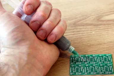
3. Ensure Uniform Solder Paste Application: Inconsistent solder paste deposition is a primary contributor to tombstoning. Uneven amounts of paste—either too much or too little on one pad—create imbalanced wetting forces.
● Refine stencil design: For 0402 components, consider using a 4-mil (0.1 mm) thick stencil with apertures sized at approximately 90% of the pad area to precisely control solder paste volume.
● Monitor paste height: Aim for a consistent paste thickness of 0.1–0.15 mm. Excessive paste (e.g., 0.2 mm) can cause components to lift during reflow.
● Utilize Automated Optical Inspection (AOI): Deploy AOI systems to detect solder paste misprints before the reflow process, preventing downstream defects and costly rework.
4. Control the Reflow Profile Meticulously: A properly tuned reflow profile is critical to ensure that solder on both pads melts simultaneously, thereby preventing the imbalances that lead to tombstoning.
● Implement a slow ramp-up rate: Maintain a preheat ramp rate of 1–2°C per second (up to 150°C) to prevent thermal shock. Rapid ramp rates (e.g., 4°C/s) can result in uneven heating.
● Incorporate a soak zone: Introduce a soak zone where the board is held at 150–180°C for 60–90 seconds. This allows temperatures to equalize across the board before reaching the peak reflow temperature (e.g., 245°C for SAC305 solder).
● Regularly calibrate your oven: A temperature variation of even 5°C across different zones within the reflow oven can trigger tombstoning. Perform regular calibration using a thermal profiler.

Component Selection and DFM Integration
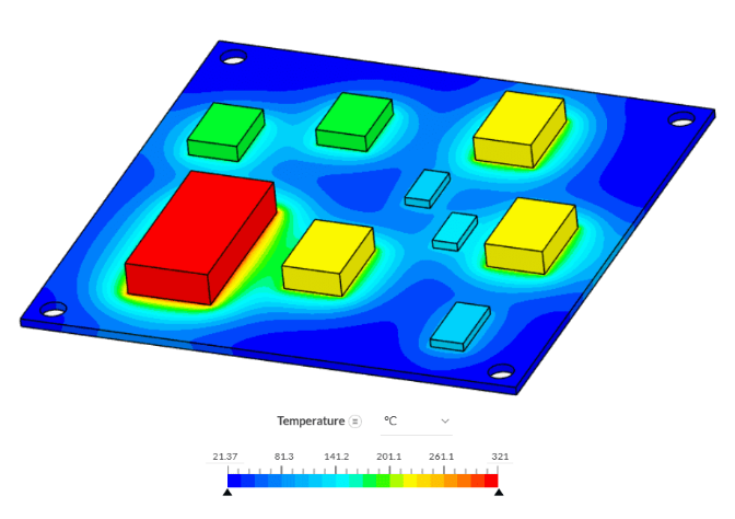
5. Balance Thermal Mass and Trace Design: Discrepancies in thermal mass, often due to varying trace widths or copper pours, can cause one pad to heat more slowly, increasing the likelihood of tombstoning.
● Symmetrize traces: If one pad connects to a 0.5 mm trace and the other to a 1 mm trace, the larger trace acts as a heat sink, delaying melting. Ensure trace widths and orientations are matched symmetrically.
● Limit adjacent copper pours: A large copper area located near one pad can reduce its heating rate by 10–15%. Utilize thermal reliefs (e.g., 0.2 mm spokes) to thermally isolate pads from large copper areas.
● Place vias judiciously: A via placed too close (e.g., 0.3 mm) to a pad can act as a heat sink. Position vias further away (>1 mm) or mirror their placement on both sides of the component.
6. Select Components and Solder Wisely: The physical characteristics of components and the type of solder used significantly influence the risk of tombstoning. Prioritize choices that enhance stability.
● Favor larger package sizes: Larger components, such as an 0603 part (1.6 mm x 0.8 mm), exhibit greater resistance to lifting compared to smaller 0201 parts due to their increased mass (approximately 2 mg vs. 0.2 mg).
● Choose plastic-range alloys: Solder alloys with a broader "plastic range," like SAC305 (melting range 217–220°C), transition from solid to liquid more gradually. This extended phase reduces the chance of wetting imbalances compared to eutectics like Sn63/Pb37, which have a sharp melt point at 183°C.
● Conduct combination testing: Always reflow a sample board using your chosen component and solder combination to identify and address potential risks early in the development cycle.
7. Implement Design for Manufacturing (DFM) Checks: Integrating DFM checks into your workflow can identify and mitigate tombstoning hazards before production begins, saving considerable time and reducing scrap.
● Simulate reflow conditions: Leverage DFM tools within software like Altium or KiCad to model heat distribution across the PCB, flagging any pads exhibiting temperature differences exceeding 10°C.
● Collaborate with assembly partners: Share your Gerber files and design specifications with your chosen PCB assembly manufacturer. Their expertise can help review pad layouts and thermal balance, offering crucial insights.
● Iterate design through prototyping: Conduct a quick prototype run to identify any latent tombstoning trends. Addressing these issues in early prototypes is far more cost-effective than rectifying them in full-scale production.
AIVON's Commitment to Flawless PCB Assembly
At AIVON, we are dedicated to helping our clients overcome complex manufacturing challenges like tombstoning. Our state-of-the-art manufacturing capabilities ensure precision at every stage, from meticulous pad fabrication to optimized reflow soldering processes. We offer quick-turn prototyping services, allowing you to swiftly test and refine your designs within days. This iterative approach enables you to fine-tune pad layouts or thermal profiles, effectively eliminating defects before committing to full-scale production. Our robust global logistics system ensures rapid delivery of your boards, while our extensive expertise in high-quality assembly—supported by advanced ENIG finishes and precisely optimized reflow processes—significantly minimizes manufacturing risks. Partnering with AIVON means you gain a dedicated team committed to transforming your designs into reliable, high-performance PCBs.
Conclusion: Mastering Tombstoning Prevention
Tombstoning does not have to be an inevitable specter haunting your PCB assembly process. By diligently optimizing pad design, judiciously selecting the appropriate surface finish, ensuring flawless solder paste application, precisely fine-tuning reflow profiles, balancing thermal mass, choosing stable components, and rigorously leveraging Design for Manufacturing (DFM) checks, you can reliably keep SMD components flat and fully functional. These proactive measures not only drastically reduce defects but also significantly boost production yields, lower overall manufacturing costs, and, most importantly, ensure that your electronic devices perform with unwavering reliability—whether they are powering a simple gadget or a critical, life-saving medical instrument. With the comprehensive insights and actionable strategies provided in this guide, you are now well-equipped to build PCBs that are designed to stand the test of time, rather than standing up on their own.