PCB Specifications
| Parameter | Value | Parameter | Value |
|---|---|---|---|
| PCB Type | FR4 PCB | Quantity | 15 pcs |
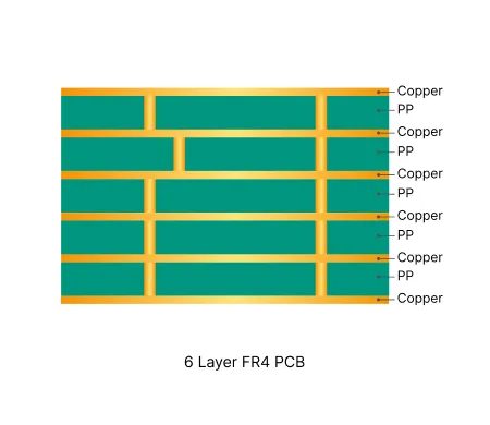
| Layers | 6 Layers | Board Type | Single PCB |
| Dimensions | 73 x 41 mm | Copper Weight | 4oz |
| Thickness | 2 mm | Min Track / Spacing | 10/10mil |
| Surface Finish | HASL Lead Free | Min Hole Size | 0.3mm↑ |
| Solder Mask | Black | Silkscreen | White |
| Stack-up | Custom | Impedance Control | No |
Manufacturing Timeline
Logistics Information
Key Manufacturing Processes
Manufacturing Summary
This production record covered a standard 4-layer FR4 PCB with heavy copper weight of 3oz on the outer layers and 2oz inner layers. Panels measured 280mm × 220mm with a finished board thickness of 2.4mm. The design specified 7/7 mil trace and spacing, 0.35mm minimum hole size, and HASL Lead Free surface finish to support elevated current requirements while maintaining standard fabrication compatibility.
Engineering review focused on plating distribution across the thick copper features. Following material preparation, inner layer imaging and circuit etching were completed before layer stack alignment and high pressure lamination. Thick copper electroplating required extended bath cycles to reach target weight, after which controlled copper etching preserved trace profiles and avoided excessive undercut on the heavier foil.
Solder mask application, molten solder coating, and hot air leveling produced a consistent surface topography suited to the board’s power delivery needs. Full electrical testing verified net continuity and isolation on every panel. The complete sequence took 11.2 days and yielded boards that met all dimensional and performance criteria without deviation.
Explore More PCB Manufacturing Resources

Real Production Records
| Order ID | PCB Type | Layers | Dimensions | Solder Mask | Surface Finish | Quantity | Action |
|---|---|---|---|---|---|---|---|
| FR4-20260528-028 | FR4 PCB | 2 | 185 x 245 | Green | HASL Lead Free | 5 | View detail |
| FR4-20260526-001 | FR4 PCB | 2 | 100 x 100 | Green | HASL Lead Free | 10 | View detail |
| FR4-20260525-001 | FR4 PCB | 2 | 50 x 45 | Matte Green | HASL Lead Free | 20 | View detail |


