The 4 Common PCB beginners Mistakes mind ruin your PCB
What This Video Covers
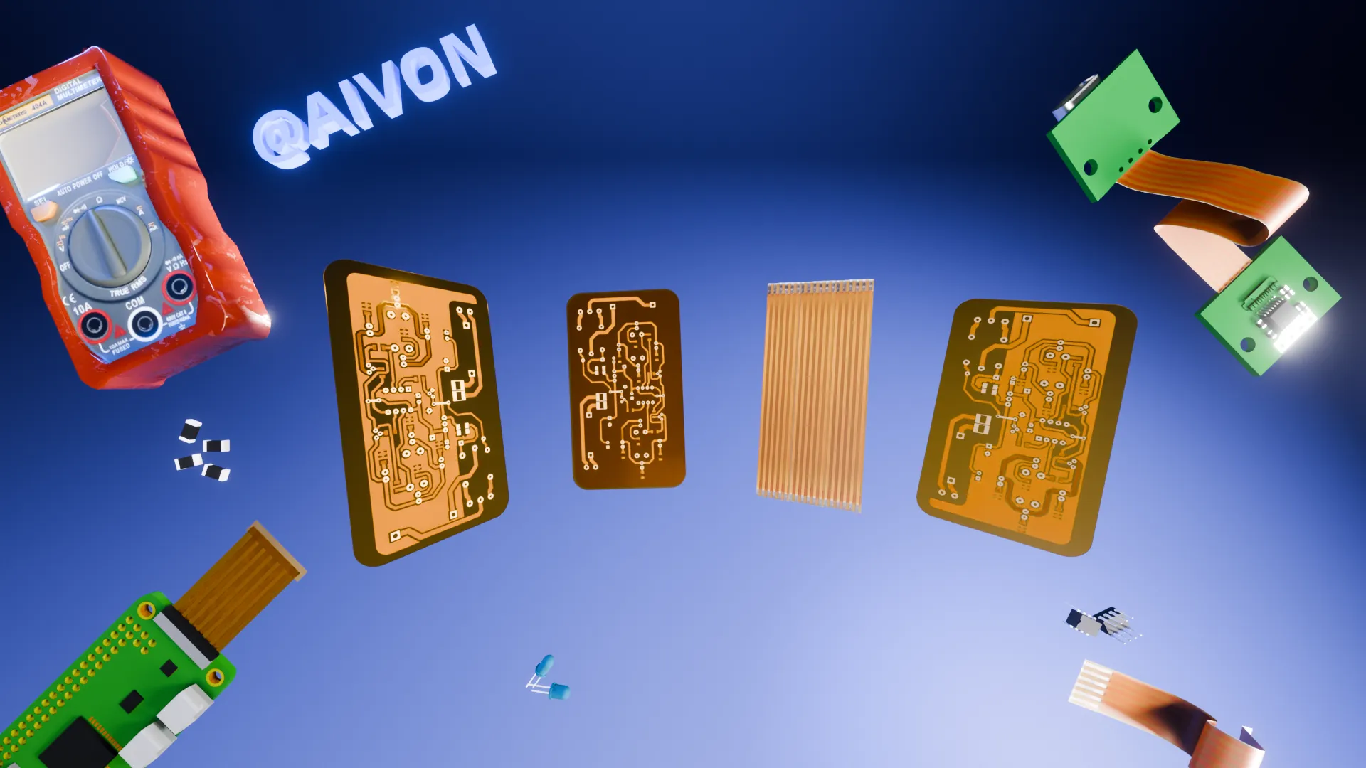
This video explains how avoiding four frequent PCB design errors saves hours of debugging, rework, and frustration for new designers and engineering teams. It covers practical tips to prevent board failures during fabrication and assembly, helping users improve workflows whether building prototypes or scaling production. The guidance applies directly to real-world projects in automotive electronics, medical devices, industrial control systems, and IoT applications where reliability is critical. Viewers learn to identify overlooked issues early, reducing risks in multilayer designs and ensuring better outcomes in demanding environments.
For instant pricing on prototypes or production runs, explore our PCB quote tool. Teams working on complex builds can also review rigid-flex PCB options and HDI PCB capabilities to apply these lessons effectively.
Key Highlights
Early detection of common design errors prevents costly debugging and rework in PCB fabrication.
Improved design workflows reduce failures in multilayer, rigid-flex, and high-density boards used in automotive and medical applications.
Actionable tips help engineers and OEM teams achieve reliable results without repeated manufacturing revisions.
FAQ
Q1: How do common PCB design mistakes increase manufacturing costs?
A1: Mistakes such as incorrect layer stack-up or inadequate trace spacing often lead to failed boards, requiring multiple fabrication and assembly iterations that raise overall project expenses.
Q2: What PCB design errors most commonly affect signal integrity in multilayer boards?
A2: Overlooked issues like improper impedance control or thermal management in multilayer PCBs can degrade performance, especially in high-frequency or automotive applications.
Q3: How can beginners avoid mistakes when ordering PCB prototypes for the first time?
A3: Reviewing design rules early and using reliable quoting tools helps prevent errors that cause delays or failures during initial prototyping and testing.
4 PCB mistakes beginners don't realize—until it's too late.
One. Laying out before the schematic is done. You're halfway through routing, then realize—oops, forgot the crystal. Every missing component later means a painful rework.
Lock your schematic first. Even a rough netlist is better than guessing.
Two: Treating power and ground as an afterthought. Treating power and ground as an afterthought.
If power is unstable, nothing else matters. Plan power and ground early. Prioritize return paths and decoupling caps.
Three:Leaving no room for debugging. No test points, no probe space, no silkscreen labels.Now you're debugging blind—with tweezers and prayers. Leave pads, headers, or even just vias.
Four:Trusting footprints without checking them.The part arrives. The pads don't match. The board's a coaster now.One wrong footprint can kill the entire board.Always cross-check: pinout, pad size, orientation, and 3D model.
This is AIVON. Check this before your next layout.