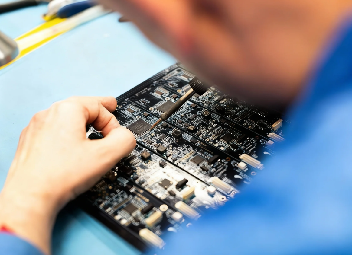
What is PCB Depanelization and Why Does it Matter?
Depanelization is the essential process of separating individual circuit boards from a larger manufacturing panel or array. This critical step directly impacts both production efficiency and the final quality of electronic products. Among the most common depanelization techniques are stamp holes (also known as mouse bites) and V-scoring (or V-cut). This article will delve into the details of stamp hole connections, examining their benefits and drawbacks, and offering a thorough comparison with V-scoring to assess their practical utility and performance in real-world applications.
Understanding Stamp Hole Connections
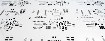
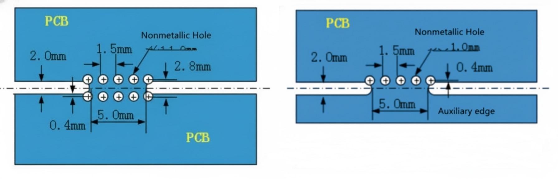
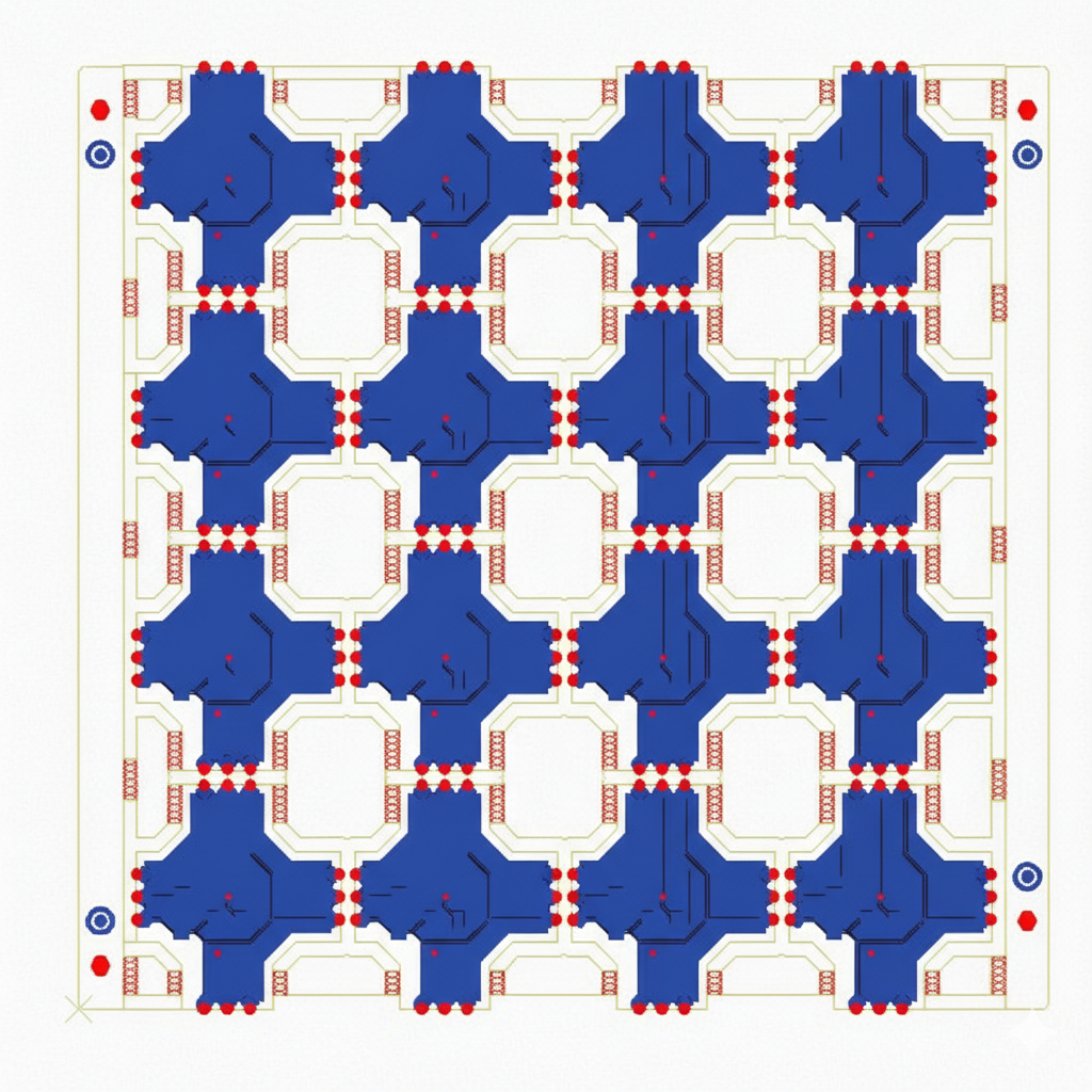
A stamp hole connection is a method of depanelization where small, perforated holes are strategically drilled along the predetermined separation lines of a circuit board panel. These tiny holes allow the individual boards to remain connected throughout the manufacturing process, providing structural integrity, yet enabling their easy separation later by either manual breaking or using a depaneling machine. The technique gets its name from its resemblance to the jagged perforations on the edge of a postage stamp, and it is frequently referred to as "mouse bites."
Design Guidelines for Stamp Holes
The effective design of stamp holes involves careful consideration of several parameters, including hole diameter, hole spacing, and the distance from the holes to the PCB's edge.
● Hole Diameter: Typically ranges from 0.6 mm to 1.0 mm. Smaller diameters (e.g., 0.6 mm) are often preferred for boards requiring higher precision and greater structural strength, while larger diameters (e.g., 1.0 mm) facilitate easier separation.
● Hole Spacing: The distance between the centers of adjacent holes usually falls between 1.0 mm and 1.5 mm. This spacing can be adjusted based on the PCB's thickness and the required panel strength. Denser spacing (e.g., 1.0 mm) is generally better suited for thinner boards, whereas wider spacing (e.g., 1.5 mm) works well for thicker substrates.
● Distance to Board Edge: This dimension is typically maintained between 0.2 mm and 0.5 mm from the edge of the individual board. This specific distance is crucial for ensuring sufficient board strength before separation while still allowing for straightforward depaneling.
What are the Benefits and Limitations of Stamp Hole Connections?
Stamp hole connections offer several distinct advantages, particularly in terms of processing ease, cost-efficiency, and design flexibility, though they do come with certain limitations.
Advantages of Using Stamp Holes
● Simplified Processing: Implementing stamp hole connections requires only an additional drilling step during PCB manufacturing, making the overall process relatively simple and easy to integrate into existing workflows.
● Lower Production Cost: Since this method avoids the need for specialized equipment beyond standard drilling machines, its implementation cost is generally lower, as it primarily involves adding a few process steps during the drilling phase.
● Reduced Depaneling Stress: The stamp hole method imparts less mechanical stress on the PCBs during separation. This characteristic makes it especially suitable for boards containing sensitive components or precision circuitry that could be damaged by higher stress methods.
● High Design Flexibility: The location and quantity of stamp holes can be customized to suit specific design needs, making this method adaptable for PCBs of various shapes and sizes, including irregular contours.
Alternative Depanelization Techniques
Beyond stamp holes, several other methods exist for depanelizing PCBs, each with unique characteristics that make them suitable for different production scenarios.
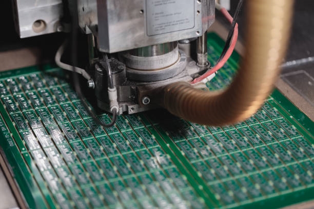
● Tab Routing: This technique involves using a CNC router to define the PCB outlines, leaving small "tab bridges" that hold the boards in the panel. These tabs are often reinforced with mouse bites for added strength. Tab routing offers precision for complex board shapes while providing robust support during handling. The tabs are removed post-assembly, typically with pliers or a punching tool.
● Laser Depanelization: Employing UV or CO2 lasers, this method cuts or ablates material to separate boards. It is particularly effective for high-density interconnect (HDI) and flexible PCBs due to its non-contact nature and extremely low mechanical stress. While it offers unparalleled precision and eliminates burrs or delamination, the initial equipment cost is high, and cutting speeds can be slower for thicker substrates.
● Automated vs. Manual Depaneling: Automated systems are favored in high-volume production for their ability to reduce operator error, increase repeatability, and ensure consistent quality. Manual depaneling, while less expensive, may not meet the stringent IPC standards required for high-reliability industries.
What is V-Scoring in PCB Depanelization?
V-scoring, also known as V-cut, is another widely used PCB depanelization method that offers distinct advantages, particularly in achieving smooth board edges and optimizing material usage.

V-Scoring Specifications and Design Recommendations
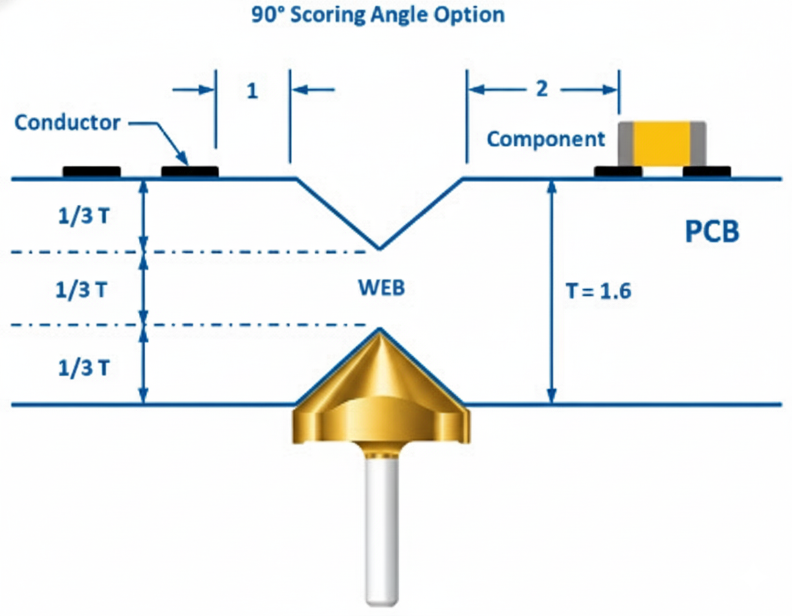
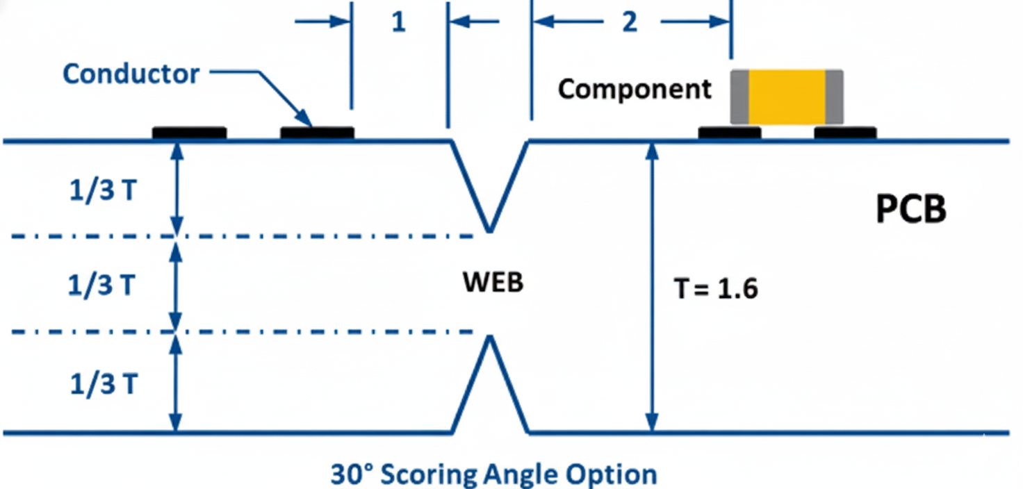
V-scoring involves cutting V-shaped grooves into the top and bottom surfaces of a PCB panel along the separation lines, leaving a thin web of material that can be easily snapped.
● Panel Boundary: It is recommended to maintain a minimum substrate boundary of 5.00 mm. For boards sharing a common outline, two parallel V-scores are typically added along the longest sides of the PCB, with no gaps left between the individual boards. The V-cut is then processed along this shared outline.
● Processing Direction: V-scoring machines only process cuts along the X and Y axes; diagonal cuts are not possible. Therefore, the board outlines requiring V-scoring must be straight lines that extend across the entire panel array.
● Scoring Depth: The typical scoring depth is approximately one-third of the total material thickness. The V-grooves are cut on both the upper and lower sides of the PCB, leaving roughly one-third of the total thickness as the remaining web material. For example, on a 1.6 mm (0.062 inches) thick board, the remaining material thickness would be around 0.53 mm (0.021 inches).
● Board Thickness Requirements: V-scoring is generally recommended for panels with a minimum board thickness of 1 mm to ensure stability during the process. However, the thickness of the inner web material can vary in practice, ranging from 0.15 mm to 0.4 mm depending on the length of the scoring line. Shorter scores (under 25 mm) might have a web thickness of 0.15 mm, while longer scores (over 100 mm) could require a web thickness of 0.4 mm. These figures serve as guidelines and should always be confirmed with your assembly house.
● Board Material: Standard PCB materials, primarily fiberglass, retain significant strength even with V-scoring. This means some flexing will occur before the scoring line breaks during separation. It's common to observe some fiberglass filaments along the separated V-scored edge, which can be smoothed by light sanding. To prevent damage during depaneling, all traces and circuit board features should be kept at least 1 mm away from the V-scoring edge. For optimal results, internal layers should also be pulled back by 1 mm from the V-score to maintain a consistent 1/3 thickness ratio across the top, middle, and bottom sections.
Advantages of V-Scoring
● Flat and Clean Edges: After depaneling, V-scored edges are notably flatter and cleaner compared to stamp hole separations. This reduces the need for secondary processing steps and improves the aesthetic and assembly quality of the final product.
● High Production Efficiency: V-scoring is well-suited for mass production environments due to its fast and straightforward mechanical operation, which significantly boosts production efficiency.
● Stable Panel Structure: Even before individual boards are separated, a V-scored panel maintains high structural integrity, which minimizes the risk of damage during handling, transportation, and automated assembly.
● Broad Adaptability: This method is adaptable to a wide range of PCB thicknesses, proving particularly effective for thicker multilayer boards.
Stamp Holes vs. V-Scoring: A Comparative Analysis
Choosing between stamp holes and V-scoring depends on a project's specific requirements, including processing complexity, cost, depaneling quality, and design flexibility.
Processing, Cost, and Quality
● Processing Complexity & Cost:
○ Stamp Hole: Simple processing, lower cost, suitable for all production volumes, especially small batches or rapid prototyping.
○ V-Scoring: More complex processing, higher equipment cost, generally more suitable for mass production.
● Depaneling Quality:
○ Stamp Hole: Tends to result in uneven or rough edges, often requiring additional trimming. Best for products where aesthetic edge quality is not a primary concern.
○ V-Scoring: Produces flat, high-quality edges, making it ideal for products with stringent cosmetic requirements.
● Depaneling Stress:
○ Stamp Hole: Imparts low stress on the board during separation, making it suitable for designs with sensitive and precision components.
○ V-Scoring: Involves higher stress during depaneling, requiring careful consideration and protection for nearby components.
Design Flexibility and Applicable Scenarios
● Design Flexibility:
○ Stamp Hole: Offers high design flexibility, adaptable to various shapes and complex layouts.
○ V-Scoring: Limited in design flexibility, primarily suitable for boards with regular, straight-line outlines and fixed layouts.
● Applicable Scenarios for Stamp Holes:
○ Small-batch or single-piece production.
○ Projects by beginners or hobbyists who do not have access to complex equipment.
○ Boards with irregular shapes that require flexible adjustment.
○ Finished products where a perfectly flat edge is not a critical aesthetic requirement.
○ Examples: Small circuit boards like Arduino expansion boards, sensor modules, or DIY electronic projects such as simple LED driver boards or audio amplifiers.
● Applicable Scenarios for V-Scoring:
○ Mass production or environments prioritizing high production efficiency.
○ Designs where the board layout is relatively regular and suits fixed, straight-line separations.
○ Finished products with high requirements for edge flatness and aesthetic quality.
The Future of PCB Depanelization and Collaboration
As electronic designs continue to increase in complexity and customer expectations for precision and efficiency grow, the future of PCB depaneling is moving towards greater automation, enhanced precision, and eco-friendly practices. Innovations such as AI-assisted routing, predictive maintenance for cutting tools, and sustainable manufacturing methods are actively redefining how PCB depaneling is performed across the industry.
Summary and AIVON Partnership
Both stamp hole connected boards and V-scoring techniques possess distinct advantages and disadvantages. In practical applications, engineers typically weigh factors such as overall custom PCB cost, desired production efficiency, critical product quality standards, and design flexibility to select the most appropriate board separation method. Close collaboration with experienced PCB manufacturers like AIVON is essential to align specific project requirements with optimal design and processing outcomes. AIVON's expertise in various depaneling methods ensures that clients achieve the best possible production results and product performance.