Why is PCB Impedance Critical for Your Designs?
PCB impedance refers to the opposition a circuit trace presents to alternating current (AC) signals, influenced by its physical dimensions, the dielectric material, and the signal frequency. In high-speed digital and radio frequency (RF) circuits, maintaining consistent impedance is paramount. Any deviation from the target impedance can cause signal reflections, leading to data corruption, interference, and degraded performance. For instance, many high-speed communication protocols, like USB, HDMI, and Ethernet, mandate a characteristic impedance of around 50 ohms to ensure optimal signal transmission.
Understanding and controlling impedance ensures that electrical signals travel cleanly and efficiently across the board, minimizing unwanted noise and timing delays. For hobbyists and engineers working on prototypes in a home lab, mastering impedance measurement is a vital step toward developing professional-grade circuit boards that perform reliably.
Essential Tools for Measuring PCB Impedance at Home
Measuring PCB impedance effectively doesn't require prohibitively expensive professional equipment. Several affordable tools can provide reliable results for home lab testing. Gathering these essentials beforehand will streamline your setup process.
What Equipment Do You Need?
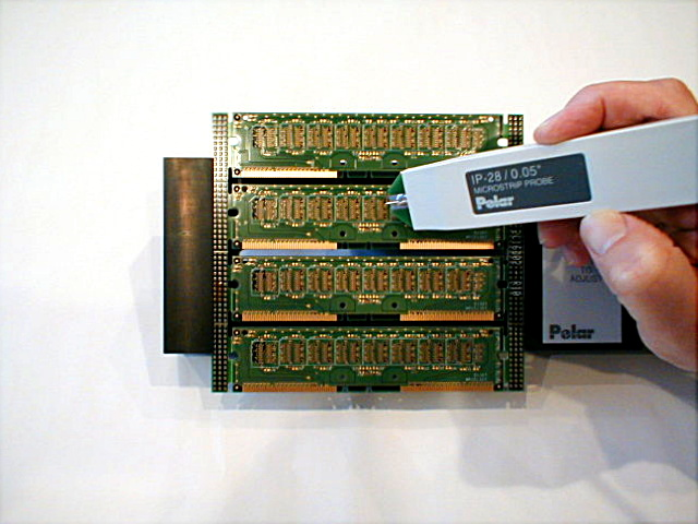
A digital oscilloscope with a bandwidth of at least 100 MHz is crucial for visualizing signal behavior. Entry-level models, typically in the 200-400 range, are often sufficient for basic impedance analysis. You’ll also need a signal generator capable of producing known signals for injecting into your PCB traces; affordable units start around $50. A basic multimeter is useful for preliminary continuity and resistance checks.To connect your equipment to the PCB, invest in reliable BNC cables and probes. Finally, a set of termination resistors (e.g., 50 ohms) is necessary to match expected impedances and absorb reflections, helping to establish a baseline. The PCB you intend to measure, ideally with accessible test points or vias, completes your setup. If budget is a concern, consider exploring borrowing options from local maker spaces or electronics clubs.
Fundamentals of PCB Impedance Measurement Techniques
Accurately assessing PCB impedance involves understanding how a trace interacts with high-frequency signals. For enthusiasts working from a home lab, the Time Domain Reflectometry (TDR) method is the most practical approach, even if you’re using basic equipment.
How Time Domain Reflectometry (TDR) Works
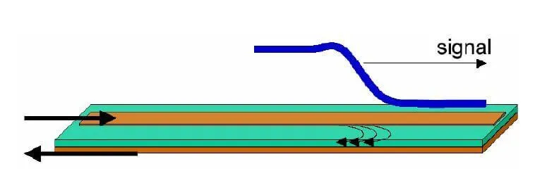
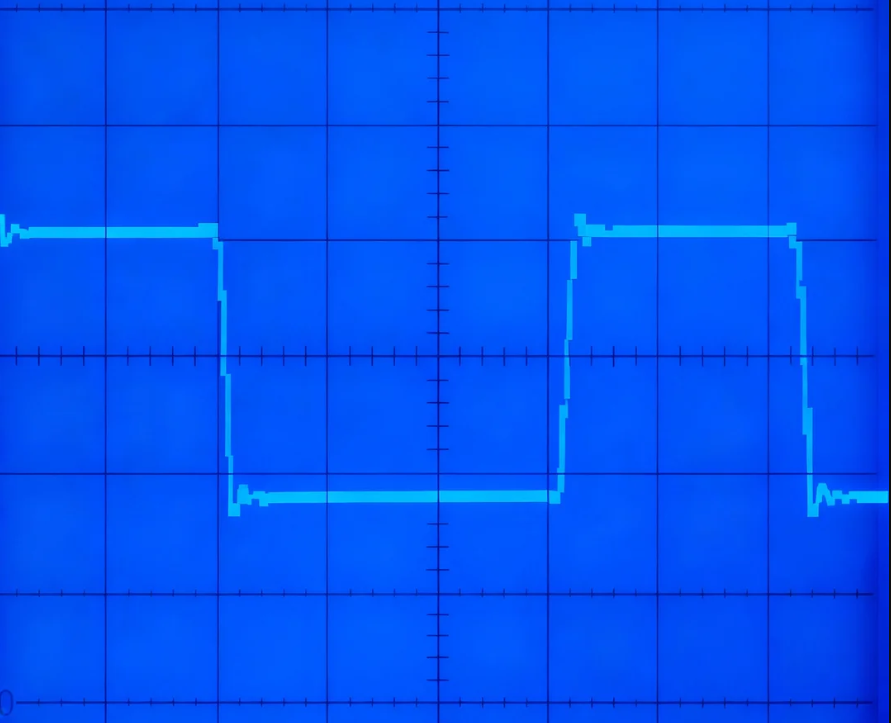
TDR operates by sending a rapid voltage pulse down a transmission line (your PCB trace) and observing any reflections that return. When this pulse encounters a change in impedance—a mismatch—part of the signal is reflected back towards the source. By analyzing the time it takes for the reflection to return and its amplitude, you can deduce the impedance profile along the trace. For example, a perfectly matched 50-ohm trace would show minimal reflection, while a sudden increase to 75 ohms would generate a noticeable reflected wave. Although professional TDR instruments are costly, an oscilloscope combined with a fast signal generator can effectively simulate this process for DIY impedance measurement.
Step-by-Step Guide to DIY PCB Impedance Measurement
Once you grasp the underlying principles, you can proceed with the practical steps to measure PCB impedance using your home lab setup. Precision in each step contributes to the accuracy of your results.
Preparing Your PCB and Test Environment
Begin by ensuring your PCB is clean and free of any debris that might interfere with electrical contact. If possible, design your board with dedicated test points or vias at the beginning and end of critical traces to simplify probe attachment. Organize your workspace to have all necessary tools within easy reach. Properly ground your entire setup to prevent noise from corrupting your measurements. Connect your signal generator to the oscilloscope using a BNC cable, and then connect a probe from the oscilloscope to the trace you wish to test.
Configuring the Signal Generator and Oscilloscope
Set your signal generator to output a square wave or a fast pulse, ideally with a rise time under 1 nanosecond. The signal frequency should be in the 1–10 MHz range, chosen based on your oscilloscope’s capabilities and the typical operating speed of signals on your PCB. For instance, testing a USB 2.0 trace might benefit from a 5 MHz signal. Initially, place a termination resistor (e.g., 50 ohms) at the far end of the trace; this helps establish a baseline by minimizing reflections.
Next, connect the oscilloscope probe to the start of your PCB trace. Adjust the oscilloscope's time scale to view the entire waveform, typically 1–10 nanoseconds per division. Set the voltage scale to capture the full amplitude of your input signal, around 1 volt peak-to-peak is often suitable. To calibrate, send a test signal through a known impedance standard (like a 50-ohm coaxial cable). Observing a clean waveform with no significant reflections confirms your setup is properly calibrated for matched impedance.
Measuring and Interpreting Reflected Signals
Remove the termination resistor from the trace's far end. Send the signal pulse from the generator and observe the oscilloscope screen for any reflected waves. The appearance of a reflection indicates an impedance mismatch. The time difference between the initial pulse and the reflected wave reveals the location of the mismatch along the trace, while the amplitude of the reflection signifies its severity.
You can approximate the characteristic impedance (Z) using the reflection coefficient (ρ): Z = Z0 * (1 + ρ) / (1 - ρ). Here, Z0 is your reference impedance (e.g., 50 ohms from your generator), and ρ is the ratio of reflected voltage to incident voltage. For example, if the incident voltage is 1V and the reflected voltage is 0.2V, ρ = 0.2, which would imply an impedance Z of approximately 75 ohms.
Analyzing Results and Iterating Your Design
Compare your measured impedance against your design’s target value. If your design aims for 50 ohms and you measure 75 ohms, adjustments to your PCB layout are likely necessary. This could involve modifying trace width or the dielectric spacing between layers during the next design iteration. Utilize online impedance calculators, inputting your PCB stack-up details (e.g., a 1.6mm FR4 board with 1oz copper), to estimate the required dimensions for your target impedance. This iterative process of measurement, analysis, and adjustment is crucial for refining your PCB design for optimal signal integrity.
Alternative Affordable Impedance Testing Methods
If a full oscilloscope and signal generator setup isn't available, other cost-effective methods can provide insights into PCB impedance, though they may offer less precision than TDR.
Using a USB Vector Network Analyzer (VNA) Dongle
Low-cost Vector Network Analyzer (VNA) dongles, often priced between $50 and $100, are increasingly popular among hobbyists. These compact devices connect to a computer via USB and can measure impedance across a wide frequency range (typically 1 MHz to 3 GHz). The accompanying software displays impedance directly, making VNAs a user-friendly option for home lab PCB testing. Follow the manufacturer’s instructions for calibration and connection to your PCB trace.
Basic Resistance Checks with a Multimeter
For extremely basic diagnostics, a multimeter can measure the DC resistance of a trace. While this method doesn't account for high-frequency effects and therefore isn't a true impedance measurement, it can help identify significant issues like open circuits or shorts. It serves as a rudimentary starting point if no other tools are accessible.
Overcoming Common Challenges in Home Lab Impedance Measurement
Conducting impedance measurements in a home lab often presents specific challenges, especially with budget equipment. Being aware of these and knowing how to address them can improve your results.
Tips for Accurate Measurements
To combat noise in measurements, ensure all components are properly grounded and keep BNC cables as short as possible to minimize interference. Avoid testing near other electronic devices that could emit electromagnetic noise. If you encounter inaccurate reflections, double-check all connections and confirm that probes are securely attached to test points; poor contact is a common culprit. When faced with limited equipment bandwidth, particularly with oscilloscopes, conduct tests at lower frequencies and interpret the results cautiously, understanding that high-frequency behavior might differ.
Enhancing Impedance Control in PCB Design
Once you've identified impedance mismatches through measurement, implementing design adjustments is key. Here are practical strategies for improving impedance control during the PCB layout phase.
Practical Design Adjustments
Adjusting trace width and spacing is fundamental: wider traces generally result in lower impedance, while narrower traces lead to higher impedance. It's crucial to maintain consistent spacing between traces and their associated ground planes. The dielectric material beneath your traces significantly impacts impedance; selecting a substrate with a known and stable dielectric constant (e.g., FR4 typically has a dielectric constant of about 4.5) is important. Finally, optimizing your layer stack-up is critical; designing boards with ground planes placed directly adjacent to signal layers helps stabilize impedance by providing a consistent return path. For example, in a 4-layer board, placing signal traces on the outer layers with ground planes immediately beneath them is a common practice.
Conclusion: Mastering Home Lab Impedance Measurement
Measuring PCB impedance at home is a valuable skill that is entirely within reach for hobbyists and engineers alike. By utilizing affordable tools and applying the techniques outlined in this guide, you can confidently perform DIY PCB impedance measurements and ensure your circuit board designs meet their performance objectives. Whether you employ an oscilloscope for TDR-like analysis or a budget-friendly VNA dongle, home lab PCB testing empowers you to tackle high-speed designs without the need for professional-grade equipment. This capability allows you to refine your skills and construct more reliable circuits directly from your own workspace.
Embrace an iterative approach: start with basic measurements, experiment with different setups, and refine your designs based on your findings. Over time, you will develop the expertise to effectively control impedance and optimize signal integrity across all your projects. This continuous learning and refinement will enable you to create PCBs that perform robustly and reliably in real-world applications.