Why is Meticulous PCB Layout Crucial for Gaming Consoles?
The printed circuit board (PCB) serves as the foundational core of any gaming console, acting as the critical interconnect for vital components such as processors, graphics chips, memory modules, and power delivery systems. A meticulously designed PCB layout is not merely an aesthetic choice; it is indispensable for ensuring superior performance, minimizing disruptive signal interference, and facilitating efficient thermal dissipation. These factors are absolutely paramount for a device expected to run graphically intensive games for extended periods.
Conversely, a poorly conceived layout can lead to significant operational issues, including input lag, severe overheating, or even catastrophic hardware failures. This comprehensive guide aims to equip designers with the knowledge to master the entire PCB layout process, guaranteeing that their gaming console designs are optimized for both peak performance and unwavering reliability, transforming a conceptual schematic into a fully functional device.
What Are the Foundational Steps in Gaming Console PCB Design?
Before delving into specific software functionalities or intricate routing strategies, it's essential to grasp the unique and demanding requirements inherent in gaming console PCB design. These devices typically manage high-speed signals, often reaching frequencies up to 5 GHz for modern graphics processing, and necessitate multiple distinct power domains (e.g., 1.2V for the CPU, 3.3V for I/O functions). Robust thermal management is also non-negotiable.
Defining Design Goals and Scope
Your layout must meticulously account for signal integrity, mitigate electromagnetic interference (EMI), and manage high component density effectively. Begin by clearly defining your design objectives: are you envisioning a compact, handheld console or a high-performance, stationary desktop system? This fundamental decision will directly influence the board size, the number of necessary layers (complex consoles often require 6-12 layers), and the specific component selection. Once this vision is solidified, you can seamlessly progress to the schematic capture phase.
Crafting the Detailed Schematic
The schematic serves as the electrical blueprint for your PCB, illustrating how all components are interconnected. For a gaming console, this will include essential elements like the central processing unit (CPU), graphics processing unit (GPU), volatile memory (RAM), storage controllers, various input/output ports (such as HDMI and USB), and sophisticated power management circuits. Utilize specialized design software to draw your schematic; widely used tools such as Altium Designer and Eagle cater to a broad spectrum of users, from novices to seasoned professionals. As you place components within the schematic, group them logically by function (e.g., power supply, processing block, connectivity interface) to simplify the subsequent layout stage.
Prioritize high-speed signals, such as those linking the CPU and GPU, ensuring they have direct connections to minimize latency. For instance, DDR memory signals often demand matched trace lengths with tight tolerances, sometimes as narrow as ±10 mils, to prevent critical timing issues. A thorough review of your schematic for any potential errors is crucial before advancing to the physical layout.
Which Software Tools Are Best for Gaming Console PCB Design?
The selection of appropriate "gaming console PCB design software" is a pivotal decision that can significantly impact the success and efficiency of your project. Two powerful options stand out for their robust capabilities in managing complex designs typical of gaming consoles.
Altium Designer: Advanced Capabilities for Complex Projects
Altium Designer is a premier choice for high-end "gaming PCB" projects, renowned for its sophisticated feature set. It offers comprehensive support for multi-layer designs, intricate high-speed signal routing, and realistic 3D visualization, all of which are critical for modern gaming consoles. Its integrated simulation tools allow for thorough testing of signal integrity and power distribution prior to manufacturing, potentially saving costly revisions. The intuitive interface facilitates a smooth transition from schematic to layout, making it an ideal solution for demanding projects with tight development cycles.
Eagle: Accessible Design for Hobbyists and Small Teams
Eagle presents another excellent option for "gaming console PCB" designs, particularly appealing to hobbyists, educational users, or smaller development teams. It boasts a user-friendly interface and extensive component libraries, though it may not offer the same depth of advanced simulation features found in more expensive, high-end tools. Eagle is perfectly suited for prototyping or for console designs that are less complex, allowing designers to concentrate on layout and routing without a steep learning curve. Both Altium Designer and Eagle support the generation of industry-standard Gerber files, ensuring seamless compatibility with PCB fabrication processes. The choice between these tools should primarily be guided by the project’s complexity, budgetary constraints, and the team’s experience level, as licensing costs can vary significantly.
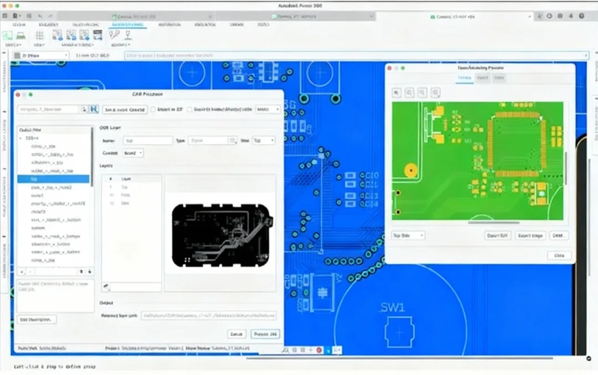
How Does One Transition from Schematic to Physical Layout?
Once your schematic is finalized, the next crucial step is to import it into the PCB editor of your chosen design software. This phase involves the physical placement of components onto the board and the creation of electrical connections between them. For a gaming console, component placement is an extremely critical process, dictated by strict space constraints and rigorous performance requirements.
Strategic Component Placement and Power Management
Begin by positioning high-priority components, such as the CPU and GPU, in central locations. This strategy minimizes trace lengths for high-speed signals, optimizing signal integrity. Power management integrated circuits (ICs) should be situated in close proximity to these core components to reduce voltage drops, ideally keeping any drop below 5% (e.g., from 1.2V to 1.14V). Decoupling capacitors (typically ranging from 0.1 µF to 1 µF) are essential and must be placed immediately adjacent to power pins to effectively filter out electrical noise and stabilize the power supply.
Defining Board Stackup and Impedance Control
Next, meticulously define your board stackup. A typical gaming console PCB often utilizes an 8-layer stackup, providing dedicated layers for power, ground, and various signal routing paths. Robust ground planes are indispensable for reducing electromagnetic interference (EMI) and establishing a stable reference for high-speed signals. For critical traces, precise impedance control is vital, targeting values such as 50 ohms for single-ended signals or 100 ohms for differential pairs, to prevent signal reflections and maintain data integrity.
What Are Best Practices for Routing Gaming Console PCBs?
The routing phase is where the true engineering challenge of a "gaming console PCB" comes to fruition. This involves creating the physical electrical connections—traces—between components while meticulously adhering to a strict set of design rules that govern signal integrity, thermal management, and manufacturability.
High-Speed Signal and Power/Ground Routing
For high-speed signals vital for data transfer between the CPU, GPU, and memory, route them primarily on inner layers with adjacent ground planes. This configuration significantly minimizes interference and provides shielding. Maintain consistent trace widths (e.g., 5-8 mils for high-speed lines) and scrupulously avoid sharp 90-degree corners, opting instead for 45-degree angles or smooth curves to prevent signal reflections and impedance discontinuities. For power and ground distribution, create robust planes to ensure stable voltage delivery. If multiple voltages are used (e.g., 1.8V for memory, 3.3V for I/O), split power planes carefully, but critically, avoid routing high-speed signals over these splits to prevent noise coupling. Utilize vias strategically to connect components to power and ground layers, ensuring low via inductance by using multiple smaller vias (e.g., 10 mil diameter) rather than a single large one.
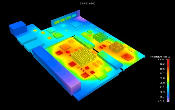
Integrated Thermal Management
Gaming consoles generate substantial heat, especially from their processors. It is crucial to incorporate thermal vias directly under high-power components to efficiently transfer heat to a dedicated copper layer or an external heatsink. Furthermore, ensure that traces in these thermally active areas are not excessively thin, as increased resistance due to heat can lead to performance degradation or even component failure. This proactive approach to thermal management is essential for maintaining long-term reliability during intense gaming sessions.
Finalizing and Validating Your Gaming Console PCB Design
Before committing your design to manufacturing, a series of rigorous checks and validations are absolutely essential to identify and rectify any potential errors. This meticulous process ensures the board's functionality, performance, and manufacturability.
Design Rule Checks and Simulation
Execute comprehensive Design Rule Checks (DRC) within your software. These checks are designed to flag issues such as overlapping traces, unconnected nets, or violations of clearance rules. For gaming consoles, set stringent clearance rules (e.g., 6 mils between traces) to prevent short circuits. Verify impedance matching for all high-speed signals and confirm that power delivery networks can adequately handle the required current demands (e.g., 2-5A for the GPU). If available, leverage simulation tools to analyze signal integrity and thermal performance. For instance, simulate crosstalk on adjacent traces, aiming for levels below -40 dB to effectively avoid interference. Address any identified issues by adjusting trace spacing, modifying routing paths, or incorporating additional shielding.
Manufacturing File Generation and Prototyping
Once the layout successfully passes all validation checks, proceed to generate the necessary manufacturing files. This typically includes Gerber files for each PCB layer (copper, silkscreen, solder mask) and a drill file for vias. Compile a comprehensive Bill of Materials (BOM) listing all components with their precise specifications. Double-check that all generated files precisely match the manufacturer's specific requirements, such as minimum trace widths (often 4-6 mils) and via sizes. Consider adding a silkscreen layer with clear labels for key components and connectors; this significantly aids in both assembly and troubleshooting, particularly for complex gaming console designs. Following manufacturing, assemble a prototype of your gaming console PCB. Conduct thorough functional testing, with a keen focus on power stability, signal timing accuracy, and overall thermal performance. Utilize an oscilloscope to measure signal rise times (ideally under 1 ns for high-speed lines) and carefully check for voltage ripple on power lines (aim for less than 50 mV). Should any issues surface, be prepared to revisit your layout, adjusting routing or component placements as necessary.
Conclusion: Bringing Your Gaming Console Vision to Life
Designing a gaming console PCB layout is a detailed and demanding process that spans from initial schematic creation to the final, intricate routing. By rigorously following this "gaming console PCB layout guide," leveraging powerful design tools like Altium Designer or Eagle, and mastering advanced PCB routing techniques, you can successfully create a high-performance board that is primed for market release. With the appropriate "gaming console PCB design software" and a disciplined, structured approach, your journey from schematic concept to a tangible, playable device will undoubtedly culminate in success.
Partner with a trusted fabrication service, such as AIVON, to transform your design into a physical reality. We are dedicated to supporting engineers with premium manufacturing solutions expertly tailored to the complex and demanding requirements of projects like gaming consoles. Embark on your design journey today and watch your innovative vision evolve into a playable, cutting-edge device!