What Are PCB Outlines and Why Are They Important?
The physical shape and exact dimensions of a printed circuit board are defined by its outline, which acts as the board's boundary. Typically, designers create this outline using specialized software on a designated "mechanical" or "board outline" layer. This crucial detail guides manufacturers, ensuring the final PCB is cut to the precise size and form required to integrate into its intended device or housing.
A well-conceived PCB outline is fundamental for several reasons. Primarily, it guarantees that the board will fit flawlessly within its product enclosure, preventing issues like component overlap or misalignment. Secondly, it provides manufacturers with critical data for accurate board cutting, minimizing material waste and reducing the risk of defective units. Finally, the board's shape can directly influence its interaction with other system elements, such as connectors or thermal management components. When planning an outline, it's vital to consider the application's spatial constraints and ensure adequate edge clearance—typically 0.5 mm to 1 mm—to protect components and traces during manufacturing and handling.
Understanding the Role of PCB Mounting Holes
Mounting holes are precisely drilled openings in a PCB, designed to secure the board to a chassis, enclosure, or other surfaces. These holes are generally larger than those for component leads or vias, often ranging from 2.5 mm to 5 mm in diameter, depending on the fastener size. Their strategic placement provides essential mechanical support, preventing movement and maintaining stability, particularly in environments prone to vibration or mechanical stress.
Beyond simply securing the board, mounting holes serve multiple critical functions. Some are plated and connected to the ground plane, effectively reducing electromagnetic interference (EMI) and improving signal integrity, especially in high-frequency circuits. In applications with significant power dissipation, holes near heat sinks can also aid in thermal management. Furthermore, they can act as alignment points during assembly, helping to ensure accurate positioning of components or connectors.
Common Types of Mounting Holes
Not all mounting holes are identical; designers choose from various types based on specific application needs and benefits.
● Plated Through-Holes (PTH): These holes feature a conductive lining, often connected to the ground plane. They are ideal when grounding or EMI shielding is a priority, helping to maintain signal integrity by mitigating noise.
● Non-Plated Through-Holes (NPTH): Lacking a conductive coating, NPTHs are used exclusively for mechanical fastening. Their simpler manufacturing process makes them a more cost-effective option for designs where electrical connectivity at the mounting point is unnecessary.
● Countersunk Holes: These holes are designed with a conical opening that allows flat-head screws to sit flush with the PCB surface. This is particularly useful for designs requiring a smooth exterior, common in compact consumer electronics.
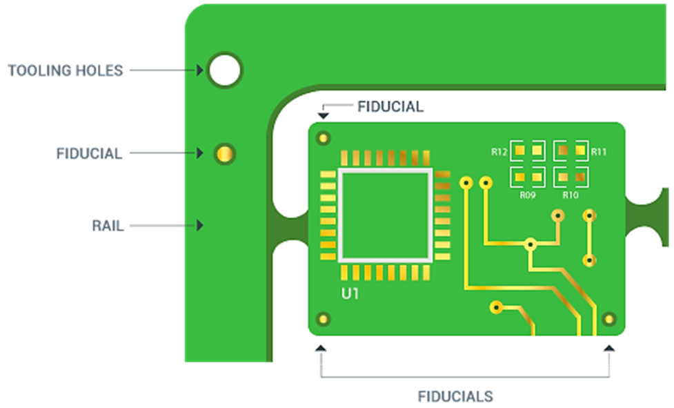
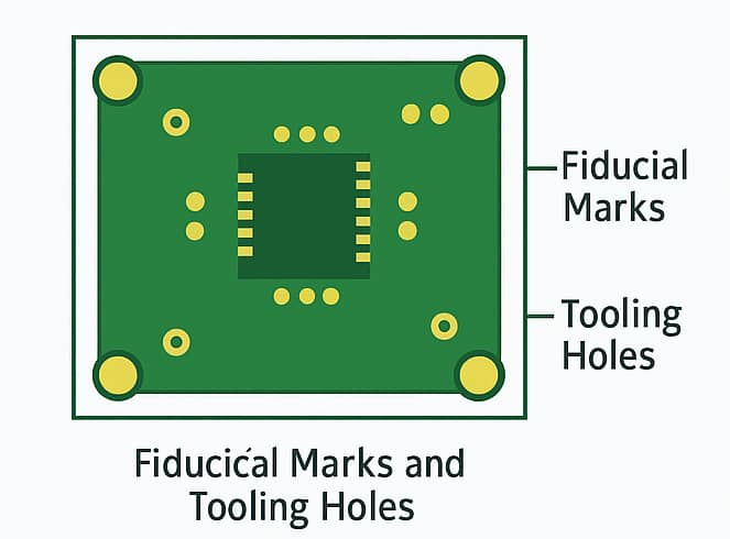
● Tooling Holes: Small and non-plated, tooling holes primarily assist manufacturing. Typically 1 mm to 1.5 mm in diameter, they are positioned away from the active circuit area and are used for machine alignment during assembly processes.
Optimizing PCB Hole Placement Strategies
Strategic placement of PCB mounting holes is crucial for ensuring mechanical stability and preventing interference with other board elements. Adhering to specific guidelines helps create a robust and reliable design.
A fundamental practice involves placing mounting holes at the corners of the PCB to provide balanced support and structural integrity. For instance, on a standard 100 mm x 50 mm rectangular board, holes might be positioned approximately 5 mm from each edge. Equally important is maintaining adequate clearance—typically 3 mm to 5 mm—between mounting holes and any nearby components or traces to avoid stress or potential damage during assembly. Designers should also strive for symmetrical hole distribution to prevent uneven stress that could lead to warping or cracking under mechanical load.
Ensuring the mounting holes align precisely with the mounting points in the enclosure is paramount. Utilizing the enclosure's design files or a 3D model during the PCB design phase can help verify this alignment. It's also wise to keep mounting holes away from high-density areas containing critical components or high-speed traces (e.g., signals operating above 100 MHz) to minimize potential interference with sensitive circuitry.
Selecting the Appropriate PCB Mounting Hardware
The choice of mounting hardware is as critical as the design of the holes themselves. Hardware must be compatible with the hole size, board thickness, and the specific demands of the application.
Common Hardware Options
● Screws and Standoffs: This is the most prevalent method for securing PCBs. Screws are typically paired with standoffs—small spacers that elevate the board from the mounting surface, ensuring adequate clearance. For a standard 1.6 mm thick PCB, M3 screws (3 mm diameter) with 5 mm to 10 mm high standoffs are often used. This configuration is highly favored when the PCB may require easy removal or replacement.
● Snap-In Clips: Offering a tool-free solution, plastic snap-in clips latch into pre-drilled holes. They are lightweight and quick to install, making them suitable for applications in low-stress environments, such as consumer gadgets.
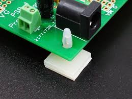
● Adhesive Pads: For temporary or very lightweight applications, adhesive pads can secure a PCB without the need for drilling. However, they are not recommended for high-vibration settings or long-term use due to potential detachment.
● Rail Systems: In industrial settings, PCBs are often mounted onto DIN rails using specialized clips or brackets. This approach is common in control systems where multiple boards need precise alignment within a rack.
When deciding on hardware, factors such as the board's weight, environmental conditions (e.g., humidity or temperature extremes), and whether the PCB needs to be easily removable should be carefully considered. For example, in automotive applications where vibrations can reach 10 G, metal screws and standoffs offer the most reliable and secure hold.
Best Practices for Robust PCB Design
Crafting a reliable PCB design demands careful attention to both the board's outline and the planning of its mounting holes. Following these actionable recommendations ensures a design that is both functional and manufacturable.
It is advisable to standardize hole sizes, such as using 3.2 mm for M3 screws, to simplify manufacturing processes and control costs. Non-standard sizes often necessitate custom tooling, which can increase production time and expenses. Furthermore, always ensure the chosen mounting hardware is appropriate for the PCB's thickness, which typically ranges from 0.8 mm to 2.4 mm; thicker boards may require longer screws or standoffs. For larger PCBs (exceeding 200 mm in any dimension), incorporating additional mounting holes toward the center helps prevent flexing, with a hole every 100 mm often effectively distributing stress.
Modern PCB design software offers robust features for defining mounting holes with specific attributes (plated or non-plated) and integrating them seamlessly into the mechanical layer alongside the outline. Always double-check the output files to confirm accuracy. Finally, before finalizing any design, it's wise to prototype the PCB and perform a test fit with the intended enclosure and hardware, as even a slight misalignment of 0.5 mm can lead to significant assembly challenges.
Avoiding Common Pitfalls in PCB Mechanical Design
Even seasoned designers can encounter missteps when it comes to defining PCB outlines and mounting holes. Being aware of these frequent errors can prevent significant delays, reduce costs, and minimize frustration throughout the development process.
A common oversight is neglecting manufacturer-specific guidelines for outline tolerances and hole sizes. Disregarding these requirements can result in boards that either do not fit their enclosures or cannot be mounted correctly. Similarly, placing mounting holes too close to the board edge (less than 2 mm) can compromise the PCB's structural integrity, potentially leading to cracks during assembly or even in everyday use. For applications where electromagnetic interference (EMI) is a concern, failing to ensure at least one mounting hole is plated and connected to the ground plane can degrade performance, particularly in high-frequency designs. Lastly, inconsistencies in defining the PCB outline across different design layers or related files can lead to critical manufacturing errors.
Mastering PCB Mechanical Design for Enhanced Product Reliability
Successful PCB design extends beyond electrical considerations; mechanical aspects, specifically the board outline and mounting holes, are equally vital for a product's success. A meticulously planned outline ensures the board integrates flawlessly into its enclosure, while carefully positioned mounting holes provide the necessary stability and grounding for dependable operation. By adopting the best practices outlined in this guide—such as placing holes strategically at corners, selecting suitable hardware, and adhering to clearance protocols—designers can produce PCBs that are both highly functional and straightforward to manufacture.
Whether the project is a small personal endeavor or a sophisticated industrial system, paying close attention to these mechanical details significantly elevates the quality of the work. Dedicate time to thoughtfully plan your board's outline, precisely position your mounting holes, and choose hardware that aligns with your application's specific demands. These steps are crucial for developing robust, professional PCB designs that offer lasting performance.