Why is PCB Layout Crucial for USB Signal Integrity?
Designing a printed circuit board (PCB) with USB interfaces demands meticulous attention to signal integrity and overall performance. A thoughtfully executed PCB layout for USB connections is instrumental in preventing data corruption, minimizing electromagnetic interference (EMI), and ensuring dependable operation.
USB interfaces are ubiquitous in modern electronics for both data transfer and power delivery. However, the high-speed nature of USB communication—ranging from 480 Mbps for USB 2.0 up to 20 Gbps for USB 3.2 Gen 2x2—renders these signals highly susceptible to noise, crosstalk, and degradation. A sub-optimal PCB layout can result in data transmission errors, diminished performance, or even complete failure of the USB link. The solution lies in optimizing your USB PCB layout. By adhering to specific USB routing guidelines and maintaining precise USB impedance control, you can guarantee that signals propagate without distortion or interference.
What Are the Core Principles for Effective USB PCB Layout?
Designing a PCB for USB interfaces necessitates careful consideration of several fundamental aspects. Here, we outline the most critical principles to guide your layout process:
Understanding USB Signal Characteristics
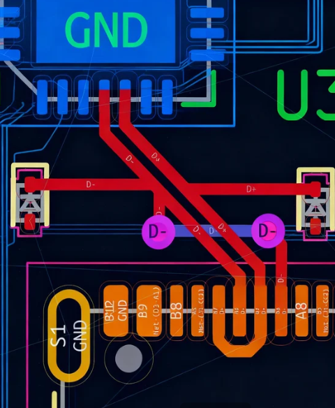
USB interfaces handle differential signals, meaning data is conveyed across two complementary traces (D+ and D- for USB 2.0, with additional pairs for USB 3.0 and beyond). These signals operate at high frequencies, so even minor mismatches or interference can lead to significant operational issues.
● USB 2.0: Functions at 480 Mbps using a single differential pair.
● USB 3.0/3.1 Gen 1: Achieves 5 Gbps, incorporating extra differential pairs for increased data rates.
● USB 3.2 Gen 2: Supports speeds up to 10 Gbps, demanding even more rigorous control over signal pathways.
● USB Type-C: Integrates high-speed data and power delivery, often supporting USB 3.2 or Thunderbolt protocols.
Comprehending the specific speed and signal type of your USB interface dictates the level of precision required in your PCB layout. Higher speeds necessitate stricter USB impedance control and shorter trace lengths to minimize signal loss.
Achieving Reliable USB Impedance Control
Impedance matching is a cornerstone of USB signal integrity. USB differential pairs typically require a characteristic impedance of 90 ohms (±15%) for USB 2.0, with tighter tolerances for USB 3.0 and higher standards. If impedance is mismatched, signal reflections can occur, leading to distortion and data errors.
To achieve proper USB impedance control:
● Utilize a PCB stack-up calculator or simulation tool to determine the correct trace width and spacing based on your board material and thickness. For example, on a standard FR-4 substrate with a 1.6 mm thickness, a trace width of approximately 0.2 mm and spacing of 0.2 mm might be necessary for a 90-ohm differential pair (exact values vary with stack-up).
● Maintain a consistent dielectric constant for your PCB material to prevent impedance variations.
● Route differential pairs over a continuous ground plane to ensure a stable reference and mitigate electromagnetic interference (EMI).
Essential USB Routing Guidelines for Optimal Trace Layout
Routing USB signals on a PCB demands precision to prevent interference and preserve signal integrity. Adhere to these USB routing guidelines to optimize your layout:
● Minimize Trace Lengths: Keep USB signal traces as short and direct as possible to reduce signal delay and attenuation. For USB 2.0, aim for lengths under 150 mm. For USB 3.0 and above, even shorter lengths (below 100 mm) are ideal.
● Ensure Equal Lengths for Differential Pairs: It is crucial that D+ and D- traces are of identical length to prevent skew, which can cause timing errors. Length mismatches should be less than 0.5 mm for USB 2.0 and even tighter for higher speeds.
● Avoid Abrupt Bends: Use 45-degree angles or smooth curves instead of sharp 90-degree bends to prevent signal reflections.
● Isolate USB Traces: Maintain a clear separation between USB traces and other high-speed or noisy signals, such as clocks or power lines, to prevent crosstalk. A separation of at least three times the trace width from other signals is recommended.
● Utilize Ground Planes: Route USB traces over a solid ground plane to provide a low-impedance return path and offer shielding against EMI.
What Advanced Techniques Enhance USB Signal Integrity?
Beyond fundamental practices, several advanced strategies can further improve USB signal integrity on your PCB. These techniques are particularly vital for high-speed USB interfaces like USB 3.0 or USB Type-C.
Strategic Via Placement
Vias introduce inductance and capacitance, which can disrupt high-speed USB signals. To minimize their impact:
● Avoid placing vias directly on USB differential pairs unless absolutely necessary. If unavoidable, use back-drilled or blind vias to reduce stub effects.
● Position vias symmetrically for both traces in a differential pair to maintain signal balance.
● Keep the number of vias per trace to a minimum—ideally fewer than two for USB 3.0 signals.
Effective Grounding and Decoupling
Proper grounding is essential for USB signal integrity. A robust ground plane beneath USB traces helps reduce noise and provides a stable reference for signals. Additionally:
● Place decoupling capacitors (e.g., 0.1 μF and 1 μF) very close to the USB controller IC pins to filter out power supply noise effectively.
● Use split ground planes only when absolutely necessary, and ensure proper stitching with vias to connect analog and digital grounds.
Shielding for USB Type-C Designs
USB Type-C connectors support both high-speed data and power delivery, making them more susceptible to interference. To optimize signal integrity:
● Implement shielding layers or enclosures around USB Type-C connectors to block external EMI.
● Route high-speed pairs (such as SuperSpeed lines) on inner layers of a multilayer PCB, sandwiched between ground planes for maximum protection.
● Ensure that appropriate termination resistors and capacitors are positioned near the connector to manage signal reflections.
What Common Mistakes Should Be Avoided in USB PCB Layout?
Even with the best intentions, certain errors can undermine your USB PCB layout. Here are some common pitfalls to be aware of:
● Ignoring Impedance Matching: Failing to accurately calculate and maintain the correct impedance for differential pairs can lead to severe reflections and data errors.
● Routing Over Split Planes: Crossing a split in the ground plane with USB traces can disrupt the signal return path and introduce significant noise.
● Uneven Trace Lengths: Mismatched lengths in differential pairs cause signal skew, which degrades performance.
● Crowding Components: Placing components too close to USB traces increases the risk of crosstalk and interference.
By being aware of these frequent mistakes, you can save considerable time and resources during your project's design and testing phases.
How Can USB PCB Layouts Be Tested and Validated?
Once your PCB layout is finalized, rigorous testing is crucial to confirm signal integrity and overall performance. Follow these steps to validate your design:
● Eye Diagram Testing: Utilize an oscilloscope to generate an eye diagram for USB signals. A clear, wide-open eye pattern indicates excellent signal integrity with minimal noise or jitter.
● Bit Error Rate (BER) Testing: Measure the BER to confirm the reliability of data transmission under various operational conditions.
● Compliance Testing: For USB certification, conduct compliance tests to ensure your design adheres to the standards established by the USB Implementers Forum (USB-IF).
Thorough testing helps identify issues that might not be apparent during the design phase, ensuring your USB interface performs as expected in real-world applications.
Conclusion: Achieving Excellence in USB PCB Layout
Crafting an effective PCB layout for USB interfaces hinges on skillfully balancing signal integrity, precise impedance control, and meticulous routing practices. By adhering to the recommended USB routing guidelines and prioritizing USB impedance control, you can effectively minimize noise, reduce signal loss, and guarantee reliable performance for your designs. Whether you are developing a straightforward USB 2.0 device or a sophisticated USB Type-C system, the core principles of USB signal integrity remain consistent: precision and an unwavering attention to detail are paramount.
Begin by thoroughly understanding the specific requirements of your chosen USB standard, then apply the best practices detailed in this guide. With careful planning, access to the right tools, and comprehensive testing, you can achieve a USB PCB layout that delivers exceptional performance and unwavering reliability for all your projects.
At AIVON, we are dedicated to supporting engineers with the resources and services necessary to bring their innovative designs to fruition. Keep these essential tips in mind for your next USB PCB project, and witness your designs elevate to new benchmarks of efficiency and quality.