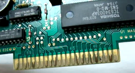
Why Are Gold Fingers Crucial for PCB Functionality?
Gold fingers, often called edge connectors, are specialized gold-plated contact pads located along the peripheral edge of a printed circuit board. Their primary role is to establish a robust electrical connection between the PCB and other electronic components, such as a motherboard, expansion card, or a module’s slot. This interface is vital for transmitting signals and power reliably.
The choice of gold for these contacts is deliberate, leveraging its superior electrical conductivity (with a typical resistivity of approximately 2.44 × 10^-8 Ω·m) and exceptional resistance to oxidation and corrosion. These properties are essential for maintaining stable signal integrity, even in demanding applications that involve high frequencies (reaching several GHz) or harsh environmental conditions, ensuring long-term operational consistency.
What Common Problems Arise with Gold Finger Plating?
Defects in the gold plating of edge connectors can severely compromise the performance and longevity of a PCB. Such issues can originate from various stages of manufacturing, environmental factors, or even initial design flaws. Understanding these common problems is the first step toward effective troubleshooting and prevention.
Peeling Gold Plating
Peeling occurs when the gold layer detaches from the underlying substrate, usually the nickel or copper layer. This manifests as visible flaking or lifting, often starting at the edges of the contact. Causes include inadequate cleaning or surface preparation before plating, which hinders proper bonding. A nickel underlayer that is too thin (ideally 3-5 micrometers) or uneven can also weaken adhesion, as can surface contaminants like oils or dust introduced during the plating process.
Corrosion and Discoloration Issues
Corrosion appears as tarnishing or pitting on the gold surface, typically resulting from a porous gold layer that fails to protect the underlying metal. If the gold plating is too thin (below 0.5 micrometers for soft gold), corrosive elements from the environment, such as high humidity or sulfur, can penetrate it. Discoloration, presenting as reddish or brownish hues instead of the expected bright gold, often indicates impurities in the plating bath, nickel diffusing to the surface due to insufficient gold thickness, or oxidation of underlying layers from excessive heat exposure.
Poor Adhesion and Inconsistent Thickness
Weak gold finger adhesion means the gold layer struggles to bond securely, making it susceptible to delamination or peeling when subjected to mechanical stress or temperature fluctuations. This can stem from an overly smooth surface lacking the necessary roughness for mechanical interlocking, incorrect plating parameters (like current density or bath temperature), or defects within the underlying copper or nickel layers. Plating thickness issues, where the gold layer is either too thin (leading to wear and corrosion) or too thick (increasing cost and risking cracking), are usually caused by inconsistent current distribution, insufficient real-time monitoring, or suboptimal PCB panel layouts.
How Can Gold Finger Plating Problems Be Resolved and Prevented?
Addressing and avoiding defects in PCB gold finger plating requires a systematic approach, combining meticulous process control with vigilant inspection and testing. By implementing best practices at every stage, manufacturers can significantly enhance the reliability of their edge connectors.
Effective Troubleshooting Strategies
For peeling issues, ensuring thorough pre-plating cleaning and micro-etching is paramount, alongside verifying nickel layer consistency (3-5 micrometers) with techniques like XRF. To combat corrosion, measure gold thickness (0.8-1.5 micrometers for hard gold, 0.5-0.8 for soft gold) and consider conformal coatings or moisture-proof storage. Discoloration can often be resolved by regularly testing and filtering the plating bath to eliminate impurities and maintaining optimal bath chemistry (e.g., pH 4.0-4.5, temperature 50-60°C). For poor adhesion, a slightly roughened surface (Ra value of 0.5-1.0 micrometers) achieved through micro-etching is beneficial, along with precise control of plating parameters. To correct thickness inconsistencies, optimize plating equipment for uniform current distribution and integrate in-process XRF monitoring.
Proactive Preventive Measures
Prevention is always more effective than correction. Strict control over plating bath conditions—including temperature, pH, and current density—is crucial for consistent quality. Using high-purity gold and nickel solutions helps prevent contamination and ensures a durable finish. Regular quality checks, such as adhesion tests (like tape testing per IPC-TM-650 standards) and thickness measurements, should be routine. Designing gold fingers with a bevel (typically 30-45 degrees) can reduce wear from repeated insertions. Finally, proper environmental protection, including anti-static, moisture-proof packaging with desiccants for storage and shipping, safeguards the gold fingers from damage.
What Methods Are Used to Inspect Gold Finger Quality?
Regular and thorough inspection, coupled with specific testing protocols, is indispensable for identifying any gold finger defects before they lead to functional failures in a finished PCB. Implementing these checks ensures that quality standards are consistently met.
Visual and Measurement Techniques
Initial visual inspection, utilizing a magnifying glass or a microscope (at 10x-20x magnification), allows for the detection of visible flaws such as discoloration, peeling, or pitting on the gold surface. Following this, precise thickness measurement is critical. Techniques like X-ray fluorescence (XRF) or coulometric testing are employed to confirm that the gold layer’s thickness (e.g., 0.5-1.5 micrometers) adheres to design specifications and industry standards.
Performance and Durability Testing
To assess the mechanical integrity and environmental resilience of the gold plating, adhesion tests are performed. These can include a tape test or thermal cycling tests, which evaluate how well the gold layer withstands physical stress and temperature variations. For rigorous assessment of corrosion resistance, salt spray testing (in accordance with MIL-STD-883 standards) is conducted. This simulates harsh environmental conditions to verify the gold layer's protective capabilities and its long-term durability in challenging operational settings.

The Path to Achieving Reliable Gold Finger Plating
Navigating the complexities of PCB gold finger plating issues—such as peeling, corrosion, discoloration, poor adhesion, and thickness inconsistencies—can be demanding, yet these challenges are entirely surmountable with the right strategies. By gaining a deep understanding of the underlying causes, implementing stringent process controls, and conducting exhaustive inspections, manufacturers can ensure that their PCBs feature dependable and robust gold fingers.
AIVON is dedicated to supporting your projects with superior manufacturing solutions specifically designed to avert these common problems and consistently deliver exceptional outcomes. Equipped with the insights from this practical guide, you now possess the essential tools to diagnose, resolve, and prevent common gold finger plating defects. Applying these recommendations to your upcoming projects will undoubtedly yield the benefits of consistently high-performance edge connectors.