PCB Specifications
| Parameter | Value | Parameter | Value |
|---|---|---|---|
| PCB Type | FR4 PCB | Quantity | 20 pcs |
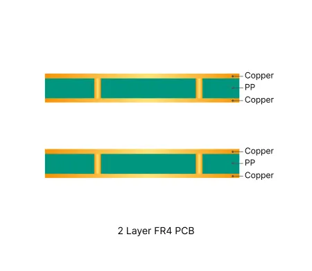
| Layers | 2 Layers | Board Type | Panel PCB |
| Dimensions | 120 x 95 mm | Copper Weight | 1oz |
| Thickness | 1.6 mm | Min Track / Spacing | 6/6mil↑ |
| Surface Finish | ENIG (Immersion Gold) | Min Hole Size | 0.3mm↑ |
| Solder Mask | Green | Silkscreen | White |
| Stack-up | Default | Impedance Control | No |
Manufacturing Timeline
Logistics Information
Key Manufacturing Processes
Manufacturing Summary
The manufacturing of these 20 panel PCBs centered on standard 2-layer FR4 construction with 1oz copper and 1.6 mm thickness. Dimensions of 120 x 95 mm together with minimum 0.3 mm holes and 6/6 mil traces followed conventional process windows during material preparation, circuit imaging, and etching. We maintained the default stackup throughout lamination to secure consistent layer alignment across the entire batch.
Green solder mask and white silkscreen were applied before surface finishing. Electroless nickel deposition and immersion gold deposition produced a uniform immersion gold ENIG finish, delivering flat pad surfaces and reliable solderability for subsequent assembly. With impedance control not required, the focus remained on plating thickness consistency and mask alignment to prevent any encroachment on exposed copper.
All panels completed electrical testing successfully, confirming net continuity and isolation within specification. The order moved from engineering review to final inspection in 3.5 days, yielding a stable set of boards that reflect predictable execution for small-quantity 2-layer ENIG panels.
Explore More PCB Manufacturing Resources
Real Production Records
| Order ID | PCB Type | Layers | Dimensions | Solder Mask | Surface Finish | Quantity | Action |
|---|---|---|---|---|---|---|---|
| FR4-20260528-028 | FR4 PCB | 2 | 185 x 245 | Green | HASL Lead Free | 5 | View detail |
| FR4-20260526-001 | FR4 PCB | 2 | 100 x 100 | Green | HASL Lead Free | 10 | View detail |
| FR4-20260525-001 | FR4 PCB | 2 | 50 x 45 | Matte Green | HASL Lead Free | 20 | View detail |


