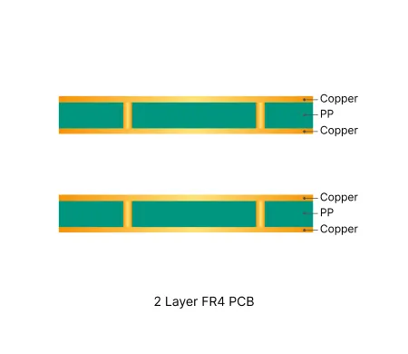
PCB Specifications
| Parameter | Value | Parameter | Value |
|---|---|---|---|
| PCB Type | FR4 PCB | Quantity | 125 pcs |
| Layers | 2 Layers | Board Type | Panel PCB |
| Dimensions | 184 x 123.8 mm | Copper Weight | 1oz |
| Thickness | 1 mm | Min Track / Spacing | 6/6mil↑ |
| Surface Finish | ENIG (Immersion Gold) | Min Hole Size | 0.3mm↑ |
| Solder Mask | Black | Silkscreen | White |
| Stack-up | Custom | Impedance Control | No |
Manufacturing Timeline
Logistics Information
Key Manufacturing Processes
Manufacturing Summary
This production record covers 125 panels of 2-layer FR4 PCB, each sized 184 × 123.8 mm with 1 mm finished thickness and 1 oz copper. The boards used a custom stackup, black soldermask, white silkscreen, and immersion gold ENIG surface finish. Minimum trace width and spacing of 6/6 mil together with 0.3 mm minimum hole size placed the design in the standard geometry range, allowing conventional process windows while still requiring careful control of panel flatness and plating uniformity across the comparatively large panel format.
We began with engineering review and material preparation, then executed circuit imaging and etching to form the conductors. Solder mask application was followed by electroless nickel deposition and immersion gold plating to produce a flat, solderable ENIG surface. Every panel received 100 % electrical testing to confirm net continuity and isolation. The full sequence was completed in 4.4 days, maintaining consistent registration and surface quality from first to last panel.
The resulting boards delivered reliable dimensional stability and finish performance suited for standard SMT assembly, meeting all specified parameters without deviation.
Explore More PCB Manufacturing Resources
Real Production Records
| Order ID | PCB Type | Layers | Dimensions | Solder Mask | Surface Finish | Quantity | Action |
|---|---|---|---|---|---|---|---|
| FR4-20260528-028 | FR4 PCB | 2 | 185 x 245 | Green | HASL Lead Free | 5 | View detail |
| FR4-20260526-001 | FR4 PCB | 2 | 100 x 100 | Green | HASL Lead Free | 10 | View detail |
| FR4-20260525-001 | FR4 PCB | 2 | 50 x 45 | Matte Green | HASL Lead Free | 20 | View detail |


