PCB Specifications
| Parameter | Value | Parameter | Value |
|---|---|---|---|
| PCB Type | FR4 PCB | Quantity | 50 pcs |
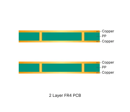
| Layers | 2 Layers | Board Type | Panel PCB |
| Dimensions | 128 x 96 mm | Copper Weight | 2oz |
| Thickness | 1.6 mm | Min Track / Spacing | 6/6mil↑ |
| Surface Finish | ENIG (Immersion Gold) | Min Hole Size | 0.8mm↑ |
| Solder Mask | Matte Green | Silkscreen | White |
| Stack-up | Custom | Impedance Control | No |
Manufacturing Timeline
Logistics Information
Key Manufacturing Processes
Manufacturing Summary
For this order of 50 panel PCBs, we manufactured 2-layer FR4 boards carrying 2oz copper on a 1.6 mm thickness with overall panel dimensions of 128 × 96 mm. The design specified a conventional 6/6 mil trace and spacing together with 0.8 mm minimum holes and a custom stackup. These parameters were processed according to the heavier copper requirements while maintaining edge definition and registration across the panels.
Engineering review and material preparation preceded circuit imaging and etching. Thick copper electroplating and controlled copper etching steps were performed to produce accurate conductor geometry on the 2oz layers. Matte green solder mask was applied and cured, followed by white silkscreen printing. The surface was then finished with electroless nickel deposition and immersion gold to form a uniform ENIG layer. Every panel received 100 % electrical testing to confirm net continuity and isolation.
The complete sequence from initial review to final inspection took 2.5 days, yielding panels with consistent solder mask coverage, sharp legend definition, and reliable ENIG surface quality. The finished boards provide the expected conductivity and protection suited to standard FR4 applications.
Explore More PCB Manufacturing Resources
Real Production Records
| Order ID | PCB Type | Layers | Dimensions | Solder Mask | Surface Finish | Quantity | Action |
|---|---|---|---|---|---|---|---|
| FR4-20260515-068 | FR4 PCB | 14 | 244 x 267 | Green | ENIG (Immersion Gold) | 10 | View detail |
| FR4-20260505-010 | FR4 PCB | 8 | 88.4 x 90.2 | Green | ENIG (Immersion Gold) | 100 | View detail |
| FR4-20260504-095 | FR4 PCB | 8 | 281 x 100 | Green | ENIG (Immersion Gold) | 10 | View detail |


