










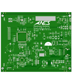
PCB Specifications
| Parameter | Value | Parameter | Value |
|---|---|---|---|
| PCB Type | FR4 PCB | Quantity | 10 pcs |
| Layers | 4 Layers | Board Type | Panel PCB |
| Dimensions | 150 x 120 mm | Copper Weight | 1oz |
| Thickness | 1.6 mm | Min Track / Spacing | 5/5mil |
| Surface Finish | HASL Lead Free | Min Hole Size | 0.25mm |
| Solder Mask | Green | Silkscreen | White |
| Stack-up | Default | Impedance Control | Yes |
Manufacturing Timeline
Logistics Information
Key Manufacturing Processes
Manufacturing Summary
This 4-layer FR-4 PCB was produced in a 10-piece run using TG130 material at 1.6mm finished thickness with 1oz copper on all layers. Measuring 150 × 120 mm, the board featured 0.25mm minimum vias, impedance control requirements, green solder mask, white silkscreen, and lead-free HASL surface finish. The design was processed as single-unit panels with standard process edges including fiducials and tooling holes.
During CAM review, several manufacturability issues required clarification, including insufficient copper clearance to V-CUT lines, tight 0.25mm via spacing that risked drill breakage, duplicate inner layer files (GP1 and G1), and pad size modifications for MBRS240LT3G diodes. These were addressed by adjusting copper features near scoring lines to prevent edge exposure, optimizing via placement for reliable drilling and plating, confirming the correct inner layer data, and verifying the revised diode footprints against annular ring and solderability requirements. Board thickness was standardized to 1.6mm ±10% for process consistency.
All engineering questions were resolved through production file revisions and customer confirmation, allowing the order to proceed without deviation from the required 11-day delivery. The finalized data package ensured stable fabrication and electrical testing results. For detailed analysis of the V-CUT clearance and via spacing resolution, refer to the full engineering case study.
Explore More PCB Manufacturing Resources
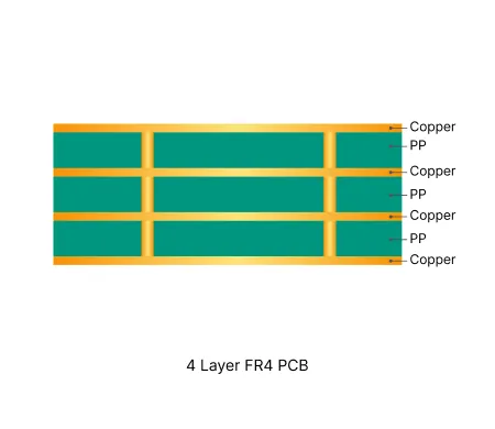
4 Layer FR4 PCB Manufacturing Insights
Standard multilayer solution offering practical routing density and controlled impedance for industrial and consumer electronics.

Multilayer FR4 PCB Engineering Queries Explained: Causes, Risks and Solutions
In-depth guide to the most frequent Engineering Queries (EQ) and DFM issues in Multilayer FR4 PCB (4/6/8+ layers) production. Real factory insights on stack-up confirmation, impedance control, copper balance, inner layer design, via treatment, registration, and practical prevention strategies.
Real Production Records
| Order ID | PCB Type | Layers | Dimensions | Solder Mask | Surface Finish | Quantity | Action |
|---|---|---|---|---|---|---|---|
| FR4-20260911-001 | FR4 PCB | 4 | 76.33 x 49.91 | Green | HASL Lead Free | 10 | View detail |
| FR4-20260910-004 | FR4 PCB | 2 | 69.92 x 69.91 | White | HASL Lead Free | 5 | View detail |
| FR4-20260907-001 | FR4 PCB | 2 | 90 x 40 | Green | HASL Lead Free | 30 | View detail |


