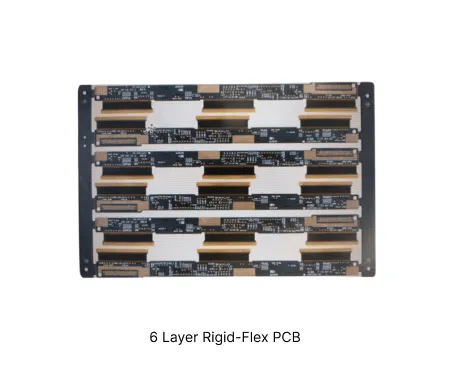
PCB Specifications
| Parameter | Value | Parameter | Value |
|---|---|---|---|
| PCB Type | Rigid-Flex PCB | Quantity | 25 pcs |
| Layers | 6 Layers | Board Type | Panel PCB |
| Dimensions | 149.1 x 209.3 mm | Copper Weight | 1OZ |
| Thickness | 1.2 mm | Min Track / Spacing | 6/6mil↑ |
| Surface Finish | ENIG (Immersion Gold) | Min Hole Size | 0.2mm |
| Solder Mask | Green | Silkscreen | White |
Manufacturing Timeline
Logistics Information
Key Manufacturing Processes
Manufacturing Summary
This order covered the production of a rigid-flex PCB with a 6-layer rigid section (1.2 mm thick, Shengyi S1150G TG155, 1 oz copper) and a 2-layer flexible section (Shengyi SF305C with yellow coverlay and white silkscreen). Key features included a 0.5 mm PI stiffener on the top layer, double-sided transparent adhesive application at the rigid-flex junction (controlled to 1.5 ± 0.5 mm width), and strict warpage control not exceeding 0.065 inches on the finished board. The design used 6 mil line/space, 0.2 mm minimum holes, ENIG surface finish, and was customer-panelized 1×4. Silkscreen requirements included date code and UL94V-0 marking placed in the flex white space, with careful adhesive point application noted for component security.
Engineering review addressed several manufacturability and reliability points. Double-sided adhesive was applied at the rigid-flex transition per the specified width to enhance bonding. The stackup was confirmed with hard board at 1.2 ± 0.12 mm and flex at 0.17 ± 0.05 mm. Inner layer copper was updated to the standard grid-plus-flow-slot pattern for better resin flow and reliability. Silkscreen was optimized by moving or knocking out characters on pads, with date code and 94V-0 markings added as required. Sharp corners were changed to R1 mm to reduce scratching risk, and stamp holes in the flex connection area were removed in favor of an octagonal shape. Four small 0.25 mm pads were enlarged to 0.3 mm with inner solder mask openings of 0.26 mm to improve solderability and process margin. All modifications were verified through updated production files.
Following these clarifications and optimizations, the boards were manufactured to specification, with controlled adhesive application, verified stackup, and compliant warpage performance. The combination of stiffener, interface adhesive, and fine DFM adjustments supported both mechanical durability and assembly requirements.
Explore More PCB Manufacturing Resources
6 Layer Rigid-Flex PCB Manufacturing Insights
Advanced 6-layer rigid-flex constructions combine mechanical stability with dynamic flexing capability for demanding electronic applications.
The Ultimate Guide to Rigid-Flex PCB Manufacturing: Mastering Complexity and Reliability at Scale
Navigate the full lifecycle of Rigid-Flex PCB Manufacturing. From solving high-density thermal challenges to scaling from prototype to production, master the tech and strategies for modern electronics.
Real Production Records
| Order ID | PCB Type | Layers | Dimensions | Solder Mask | Surface Finish | Quantity | Action |
|---|---|---|---|---|---|---|---|


