4 Layer Rigid-Flex PCB Production Record #RFP-20260427-074

| Parameter | Value | Parameter | Value |
|---|---|---|---|
| PCB Type | Rigid-Flex PCB | Quantity | 260 pcs |
| Layers | 4 Layers | Board Type | Panel PCB |
| Dimensions | 131.97 x 115.05 mm | Copper Weight | 1OZ |
| Thickness | 1.6 mm | Min Track / Spacing | 6/6mil↑ |
| Surface Finish | ENIG (Immersion Gold) | Min Hole Size | 0.3mm↑ |
| Solder Mask | Green | Silkscreen | White |
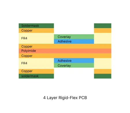
This 4-layer rigid-flex PCB (131.97 × 115.05 mm) was manufactured as 260 pieces (65 sets) with a hybrid construction: rigid sections using Shengyi S1150G TG155 FR-4 material at 1.6 mm thickness with 1 oz copper, and flex sections using Shengyi SF305C polyimide at 0.08 mm with 1/3 oz copper. The design incorporated 0.3 mm holes, 6 mil line width/space, ENIG surface finish, yellow coverlay on flex areas, green solder mask on rigid areas, and 2×2 panelization with V-CUT depanelization. Production was completed in 25 days with full flying probe testing and delivery of electrical test reports plus quality certificates.
DFM review focused on rigid-flex transition challenges. Tight edge clearances risked exposed copper and pad damage during routing; these were accepted with customer confirmation. Stamp hole and routing slot widths were standardized at 2.5 mm for reliable depanelization. Stack-up was verified to achieve target thicknesses (1.6 ±0.16 mm rigid, 0.12 ±0.05 mm flex). Via plugging followed the VIA PLUG layer where specified, while other vias received standard tenting. Silkscreen placement was adjusted to maintain minimum 0.2 mm clearance from pads, with overlapping characters removed. Process edges received inner layer glue dots, outer layer grid copper, and R1.0 mm corner chamfers for handling stability. Solder mask outline openings were tightened to 0.2 mm to prevent white edges.
All clarifications were resolved before production. The delivered boards met IPC Class III standards with consistent plating, reliable rigid-flex transitions, and clean edges. For detailed resolution of the rigid-flex stack-up confirmation and edge clearance handling in this build, refer to the related engineering case.
| Order ID | PCB Type | Layers | Dimensions | Solder Mask | Surface Finish | Quantity | Action |
|---|---|---|---|---|---|---|---|
| RFP-20260401-039 | Rigid-Flex PCB | 4 | 138 x 128 | Green | ENIG (Immersion Gold) | 5 | View detail |
| RFP-20260312-007 | Rigid-Flex PCB | 4 | 46 x 16 | Green | ENIG (Immersion Gold) | 20 | View detail |
| RFP-20251223-007 | Rigid-Flex PCB | 4 | 133.69 x 160.84 | Matte Black | ENIG (Immersion Gold) | 10 | View detail |