PCB Specifications
| Parameter | Value | Parameter | Value |
|---|---|---|---|
| PCB Type | Flexible PCB | Quantity | 1000 pcs |
| Layers | 2 Layers | Board Type | Single PCB |
| Dimensions | 10.5 x 33 mm | Copper Weight | 1/2OZ |
| Thickness | 0.13 mm | Min Track / Spacing | 6/6mil↑ |
| Surface Finish | ENIG (Immersion Gold) | Min Hole Size | 0.3mm↑ |
| Solder Mask | Yellow | Silkscreen | White |
| Material | Rolled Copper | Stiffener | PI Stiffener |
Manufacturing Timeline
Logistics Information
Key Manufacturing Processes
Manufacturing Summary
This production run for 1000 units of 2-layer flexible PCBs utilized 0.13 mm thick polyimide material with rolled copper weighing 1/2 oz. Each board measures 10.5 x 33 mm and incorporates PI stiffeners in specific zones to provide localized rigidity. The specifications called for a standard 6/6 mil trace width and spacing with minimum hole sizes of 0.3 mm, paired with yellow solder mask and white silkscreen printing.
During manufacturing, particular attention was given to polyimide material handling and coverlay lamination to preserve the thin flexible substrate integrity. Circuit imaging and etching were followed by solder mask application and the ENIG surface finish, achieved through electroless nickel deposition and immersion gold plating. To validate durability, we performed dynamic flex testing along with AOI inspection and full electrical testing on the completed circuits.
The entire order was executed over a period of 14.5 days, resulting in uniform quality and reliable performance characteristics across all boards delivered.
Explore More PCB Manufacturing Resources
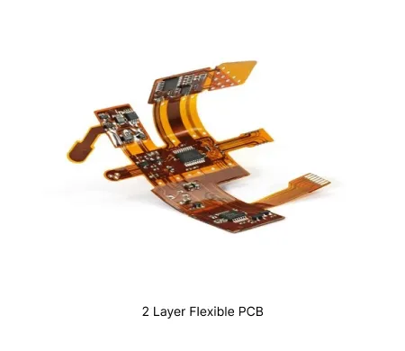
2 Layer Flexible PCB Manufacturing Insights
These circuits deliver reliable interconnects where space constraints and repeated bending demand thin, lightweight constructions with two copper layers.
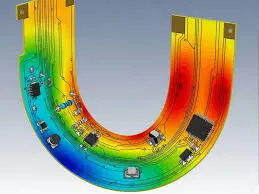
Engineering Queries in 2 Layer Flexible PCB Fabrication and Production
Explore engineering queries (EQ) in 2 layer flexible PCB manufacturing, including key DFM challenges such as bend design, coverlay alignment, via reliability, and copper balance. Practical insights help improve flexibility performance and production yield.
Real Production Records
| Order ID | PCB Type | Layers | Dimensions | Solder Mask | Surface Finish | Quantity | Action |
|---|---|---|---|---|---|---|---|
| FPC-20260707-032 | Flexible PCB | 4 | 157.2 x 38.6 | Yellow | ENIG (Immersion Gold) | 125 | View detail |
| FPC-20260526-023 | Flexible PCB | 4 | 50 x 75 | Black | ENIG (Immersion Gold) | 5 | View detail |
| FPC-20260516-042 | Flexible PCB | 3 | 76.2 x 457.2 | Yellow | ENIG (Immersion Gold) | 5 | View detail |


