PCB Specifications
| Parameter | Value | Parameter | Value |
|---|---|---|---|
| PCB Type | FR4 PCB | Quantity | 5 pcs |
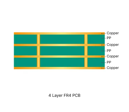
| Layers | 4 Layers | Board Type | Panel PCB |
| Dimensions | 78 x 123 mm | Copper Weight | 1oz |
| Thickness | 0.8 mm | Min Track / Spacing | 4/4mil |
| Surface Finish | ENIG (Immersion Gold) | Min Hole Size | 0.2mm |
| Solder Mask | Green | Silkscreen | White |
| Stack-up | Default | Impedance Control | No |
Manufacturing Timeline
Logistics Information
Key Manufacturing Processes
Manufacturing Summary
This production record covers five 4-layer FR4 panel PCBs measuring 78 × 123 mm with a finished thickness of 0.8 mm and 1 oz copper throughout. The design specified 4/4 mil minimum track and spacing, 0.2 mm minimum hole size, green soldermask, white silkscreen, and immersion gold ENIG finish on a default stackup. These parameters combine a thin profile with tighter geometry, requiring exact process control during multilayer fabrication while maintaining standard FR4 material properties.
We performed inner layer imaging and circuit etching to resolve the 4 mil features, followed by precise layer stack alignment and high pressure lamination calibrated for the 0.8 mm thickness to preserve registration and flatness. Solder mask application was succeeded by electroless nickel deposition and immersion gold deposition, producing a uniform ENIG surface suitable for assembly. The entire sequence from material preparation through final electrical testing was executed without deviation from the defined parameters.
All five panels passed continuity and isolation testing, confirming consistent electrical performance across the batch. The order was completed in 5.5 days, delivering reliable boards that matched the customer’s specifications for this small-quantity, fine-feature run.
Explore More PCB Manufacturing Resources

Real Production Records
| Order ID | PCB Type | Layers | Dimensions | Solder Mask | Surface Finish | Quantity | Action |
|---|---|---|---|---|---|---|---|
| FR4-20260520-046 | FR4 PCB | 2 | 94.21 x 275 | Green | ENIG (Immersion Gold) | 75 | View detail |
| FR4-20260515-068 | FR4 PCB | 14 | 244 x 267 | Green | ENIG (Immersion Gold) | 10 | View detail |
| FR4-20260506-017 | FR4 PCB | 6 | 55 x 41.7 | Green | ENIG (Immersion Gold) | 15 | View detail |


