PCB Specifications
| Parameter | Value | Parameter | Value |
|---|---|---|---|
| PCB Type | FR4 PCB | Quantity | 10 pcs |
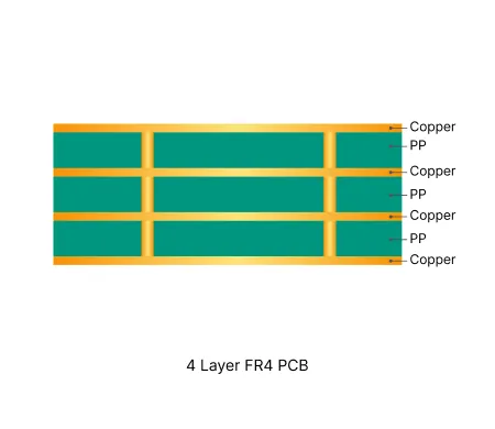
| Layers | 4 Layers | Board Type | Panel PCB |
| Dimensions | 110 x 90 mm | Copper Weight | 1oz |
| Thickness | 1.6 mm | Min Track / Spacing | 6/6mil↑ |
| Surface Finish | ENIG (Immersion Gold) | Min Hole Size | 0.2mm |
| Solder Mask | Matte Green | Silkscreen | White |
| Stack-up | Default | Impedance Control | No |
Manufacturing Timeline
Logistics Information
Key Manufacturing Processes
Manufacturing Summary
This order required fabrication of 10 panels for a standard 4-layer FR4 PCB. Each panel measured 110 x 90 mm with a finished thickness of 1.6 mm and 1 oz copper weight on all layers. The minimum feature size stayed at 6/6 mil for track and spacing, paired with 0.2 mm holes, while the surface combined matte green soldermask, white silkscreen, and immersion gold ENIG. These choices suited typical assembly needs without calling for advanced controls such as impedance matching.
Production began with engineering review and material preparation before moving into inner layer imaging, circuit etching, and accurate stack alignment. High pressure lamination bonded the layers reliably, after which we applied the soldermask and performed electroless nickel deposition followed by immersion gold. Electrical testing validated connectivity across all panels.
Completed over 11.3 days, the run delivered panels fully aligned with the provided specifications. Consistent processing at each stage supported dependable quality suitable for standard electronic applications.
Explore More PCB Manufacturing Resources

Real Production Records
| Order ID | PCB Type | Layers | Dimensions | Solder Mask | Surface Finish | Quantity | Action |
|---|---|---|---|---|---|---|---|
| FR4-20260520-046 | FR4 PCB | 2 | 94.21 x 275 | Green | ENIG (Immersion Gold) | 75 | View detail |
| FR4-20260515-068 | FR4 PCB | 14 | 244 x 267 | Green | ENIG (Immersion Gold) | 10 | View detail |
| FR4-20260506-017 | FR4 PCB | 6 | 55 x 41.7 | Green | ENIG (Immersion Gold) | 15 | View detail |


