PCB Specifications
| Parameter | Value | Parameter | Value |
|---|---|---|---|
| PCB Type | FR4 PCB | Quantity | 20 pcs |
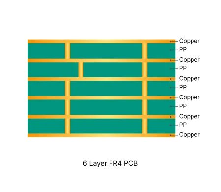
| Layers | 6 Layers | Board Type | Panel PCB |
| Dimensions | 131 x 170 mm | Copper Weight | 1oz |
| Thickness | 1.6 mm | Min Track / Spacing | 4/4mil |
| Surface Finish | ENIG (Immersion Gold) | Min Hole Size | 0.2mm |
| Solder Mask | Green | Silkscreen | White |
| Stack-up | Default | Impedance Control | No |
Manufacturing Timeline
Logistics Information
Key Manufacturing Processes
Manufacturing Summary
This record documents the production of a standard 4-layer FR4 PCB batch with immersion gold ENIG finish. The order comprised 85 panels of 125 x 85 mm boards at 1.6 mm thickness, using 1 oz copper throughout. Minimum track and spacing followed a conventional 6 mil geometry, while impedance controlled traces on inner layers added a layer of precision to the stack-up and required specific dielectric considerations during lamination.
We initiated the run with engineering review and material preparation using TG150 FR4. Inner layer imaging, etching, and accurate layer registration preceded high pressure lamination. Following solder mask application, electroless nickel deposition and immersion gold deposition were performed under controlled conditions to achieve uniform coverage and avoid nickel corrosion risks on the impedance controlled PCB.
Subsequent electrical testing validated all circuits, confirming the boards performed to specification with no opens or shorts. Completed in 15.9 days, the process yielded consistent boards ready for reliable assembly and long-term field performance.
Explore More PCB Manufacturing Resources

Real Production Records
| Order ID | PCB Type | Layers | Dimensions | Solder Mask | Surface Finish | Quantity | Action |
|---|---|---|---|---|---|---|---|
| FR4-20260515-068 | FR4 PCB | 14 | 244 x 267 | Green | ENIG (Immersion Gold) | 10 | View detail |
| FR4-20260505-010 | FR4 PCB | 8 | 88.4 x 90.2 | Green | ENIG (Immersion Gold) | 100 | View detail |
| FR4-20260504-095 | FR4 PCB | 8 | 281 x 100 | Green | ENIG (Immersion Gold) | 10 | View detail |


