PCB Specifications
| Parameter | Value | Parameter | Value |
|---|---|---|---|
| PCB Type | FR4 PCB | Quantity | 5 pcs |
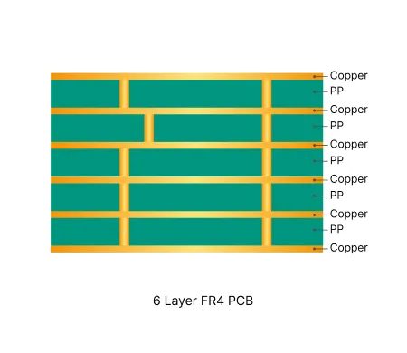
| Layers | 6 Layers | Board Type | Panel PCB |
| Dimensions | 494.3 x 247.8 mm | Copper Weight | 1oz |
| Thickness | 1.6 mm | Min Track / Spacing | 6/6mil↑ |
| Surface Finish | HASL Lead Free | Min Hole Size | 0.3mm↑ |
| Solder Mask | Red | Silkscreen | White |
| Stack-up | Default | Impedance Control | No |
Manufacturing Timeline
Logistics Information
Key Manufacturing Processes
Manufacturing Summary
This order consisted of a standard 4-layer FR4 PCB produced in panels. The boards featured 1.6 mm overall thickness with 1 oz copper on all layers and minimum 6 mil trace width and spacing. These parameters align with conventional manufacturing specifications, enabling efficient processing without requiring advanced geometry controls. During engineering review, we confirmed the stackup and drill requirements before moving into material preparation and inner layer imaging.
Layer stack alignment received particular attention prior to high pressure lamination to maintain registration accuracy across the four layers. Solder mask was applied in standard green color, after which we performed molten solder coating and hot air leveling to achieve a uniform HASL Lead Free finish. This surface treatment supports excellent component attachment while remaining cost-effective for the build quantity.
All boards underwent comprehensive electrical testing to validate circuit integrity. The complete production sequence, from initial review to final output, spanned 3.8 days while delivering consistent results that meet IPC Class 2 standards. This execution reflects the reliable processes used for multilayer boards with HASL Lead Free surface finish.
Explore More PCB Manufacturing Resources

Real Production Records
| Order ID | PCB Type | Layers | Dimensions | Solder Mask | Surface Finish | Quantity | Action |
|---|---|---|---|---|---|---|---|
| FR4-20260528-028 | FR4 PCB | 2 | 185 x 245 | Green | HASL Lead Free | 5 | View detail |
| FR4-20260526-001 | FR4 PCB | 2 | 100 x 100 | Green | HASL Lead Free | 10 | View detail |
| FR4-20260525-001 | FR4 PCB | 2 | 50 x 45 | Matte Green | HASL Lead Free | 20 | View detail |


