PCB Specifications
| Parameter | Value | Parameter | Value |
|---|---|---|---|
| PCB Type | FR4 PCB | Quantity | 5 pcs |
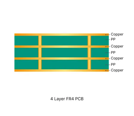
| Layers | 4 Layers | Board Type | Panel PCB |
| Dimensions | 299.5 x 208 mm | Copper Weight | 1oz |
| Thickness | 1.6 mm | Min Track / Spacing | 6/6mil↑ |
| Surface Finish | ENIG (Immersion Gold) | Min Hole Size | 0.2mm |
| Solder Mask | Green | Silkscreen | White |
| Stack-up | Custom | Impedance Control | No |
Manufacturing Timeline
Logistics Information
Key Manufacturing Processes
Manufacturing Summary
This 4-layer FR-4 board measured 299.5 × 208 mm with 1 oz copper on inner and outer layers and a standard 1.6 mm finished thickness using KB-6160 TG130 material. Produced in a quantity of 30 pieces as 2×3 customer-panelized arrays with V-cut and routing separation, the design featured 6 mil line/space, ENIG surface finish, and no process edges. No impedance control, blind vias, or resin plugging was required, with mechanical forming and 100% flying probe testing.
DFM review addressed several file and manufacturability concerns. Hole-to-copper spacing violations were resolved by reducing specific hole diameters by 0.05 mm to maintain adequate clearance without compensation. Vias in single-sided pads on the DBR1 layer were processed as non-plated holes. Silkscreen characters fell below the 0.72 mm minimum height, particularly over pads, leading to acceptance of potential incomplete or fuzzy marking. Multiple production file versions were confirmed prior to release. hole size adjustment for copper clearance ensured reliable isolation while preserving design intent and avoiding shorts.
Production completed within the short 4-day turnaround, with all boards meeting dimensional, electrical, and plating specifications. The customer-panelized configuration without process edges required careful handling but delivered consistent results suitable for assembly.
Explore More PCB Manufacturing Resources
4 Layer FR4 PCB Manufacturing Insights
Standard multilayer solution offering practical routing density and controlled impedance for industrial and consumer electronics.

Multilayer FR4 PCB Engineering Queries Explained: Causes, Risks and Solutions
In-depth guide to the most frequent Engineering Queries (EQ) and DFM issues in Multilayer FR4 PCB (4/6/8+ layers) production. Real factory insights on stack-up confirmation, impedance control, copper balance, inner layer design, via treatment, registration, and practical prevention strategies.
Real Production Records
| Order ID | PCB Type | Layers | Dimensions | Solder Mask | Surface Finish | Quantity | Action |
|---|---|---|---|---|---|---|---|
| FR4-20260520-046 | FR4 PCB | 2 | 94.21 x 275 | Green | ENIG (Immersion Gold) | 75 | View detail |
| FR4-20260515-068 | FR4 PCB | 14 | 244 x 267 | Green | ENIG (Immersion Gold) | 10 | View detail |
| FR4-20260506-017 | FR4 PCB | 6 | 55 x 41.7 | Green | ENIG (Immersion Gold) | 15 | View detail |


