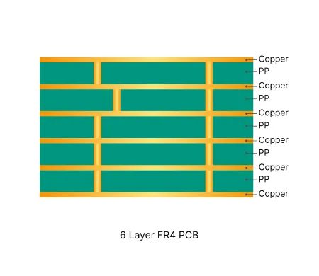
6 Layer FR4 PCB Production Record #FR4-20260418-085
| Parameter | Value | Parameter | Value |
|---|---|---|---|
| PCB Type | FR4 PCB | Quantity | 15 pcs |
| Layers | 6 Layers | Board Type | Panel PCB |
| Dimensions | 32 x 46 mm | Copper Weight | 1oz |
| Thickness | 1 mm | Min Track / Spacing | 6/6mil↑ |
| Surface Finish | ENIG (Immersion Gold) | Min Hole Size | 0.1mm |
| Solder Mask | Green | Silkscreen | White |
| Stack-up | Custom | Impedance Control | No |
This 6-layer HDI PCB was produced on 1.0mm FR-4 S1000H TG150 material with 0.5oz/1oz copper weight and ENIG surface finish. The board measures 32×46mm with 0.1mm minimum holes, 6mil line width/spacing, and 2-stage HDI construction featuring blind vias. A total of 15 pieces (5 sets) were fabricated using a customer-updated Gerber that required complete stackup redesign to JP06101H-3313A2. Production followed standard 21-day lead time with 100% flying probe testing and mechanical routing via stamp holes.
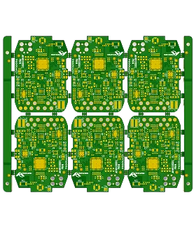
Key DFM challenges centered on solder mask bridge integrity and via handling. Multiple SMD pads showed spacing below 5.9mil process capability, risking incomplete solder mask coverage. BGA vias specified at 0.1mm were enlarged to 0.2mm to ensure reliable drilling and maintain adequate pad area for assembly. Inner layer copper density was notably low in L3, prompting auxiliary copper balancing on process edges to prevent resin starvation and warpage during lamination. Non-functional pads were removed where electrically safe, and all unopened vias received solder mask plugging per specification. Panelization was optimized from the original 1×3 layout to 3×2 configuration to reduce material waste while maintaining 10mm process margins and R2.0mm corner protection.
Stackup confirmation and solder mask bridge and BGA via adjustments were finalized after multiple EQ rounds, with blind via dimple controlled to ≤25μm. Final boards met IPC Class 2 standards with stable electrical performance and acceptable bow/twist. All units passed functional testing and were shipped with performance reports and quality certificates.
| Order ID | PCB Type | Layers | Dimensions | Solder Mask | Surface Finish | Quantity | Action |
|---|---|---|---|---|---|---|---|
| FR4-20260515-068 | FR4 PCB | 14 | 244 x 267 | Green | ENIG (Immersion Gold) | 10 | View detail |
| FR4-20260505-010 | FR4 PCB | 8 | 88.4 x 90.2 | Green | ENIG (Immersion Gold) | 100 | View detail |
| FR4-20260504-095 | FR4 PCB | 8 | 281 x 100 | Green | ENIG (Immersion Gold) | 10 | View detail |