PCB Specifications
| Parameter | Value | Parameter | Value |
|---|---|---|---|
| PCB Type | FR4 PCB | Quantity | 10 pcs |
| Layers | 4 Layers | Board Type | Panel PCB |
| Dimensions | 210 x 100 mm | Copper Weight | 1oz |
| Thickness | 1 mm | Min Track / Spacing | 4/4mil |
| Surface Finish | OSP | Min Hole Size | 0.1mm |
| Solder Mask | Green | Silkscreen | White |
| Stack-up | Custom | Impedance Control | No |
Manufacturing Timeline
Logistics Information
Key Manufacturing Processes
Manufacturing Summary
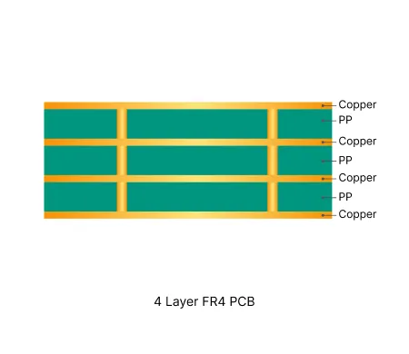
This 4-layer FR-4 PCB was produced as a 10-piece run of single boards measuring 210 × 100 mm with a finished thickness of 1.0 mm. Built with 1 oz copper on both inner and outer layers using TG130 material (substituted with equivalent TG150 due to inventory availability of the specified KB-6160), the design featured 0.1 mm minimum holes, OSP surface finish, blind vias, and green solder mask with white legend. One HDI stage was implemented, along with via tenting and selective solder mask window requirements.
DFM review uncovered multiple conflicts requiring clarification. Small SMD pads below 7.87 mil created flying probe testing difficulties that could result in undetected open/short circuits; BGA pads were non-solder mask defined, risking pad lift or solder joint cracking during assembly. Character frames positioned too close to BGA pads risked ink buildup causing component floating and cold solder joints. Process edge design with sharp right-angle corners increased risk of damaging dry film and packaging during handling and shipment. Surface finish instructions conflicted between lead-free HASL and full-board OSP, with single-side via windows potentially trapping solder balls if HASL were used. Material substitution, solder mask versus paste layer mismatches, via cover-oil versus double-side window designs, and unclear GM/GM2 layer requirements plus marking content were also resolved through iterative communication. Factory-proposed process parameters (including ±0.75% bow/twist control, tear-drop addition, non-functional pad removal on inner layers, and optimized routing) were confirmed to balance manufacturability without altering net connectivity.
After customer confirmation on OSP surface finish, selective via tenting, updated Gerber alignment for mask/paste layers, process edge treatment, and material equivalence, production proceeded smoothly. The order was completed within the 21-day window, passed 100% flying probe testing with added traceability markings, and met all dimensional, plating, and visual requirements.
Explore More PCB Manufacturing Resources

Real Production Records
| Order ID | PCB Type | Layers | Dimensions | Solder Mask | Surface Finish | Quantity | Action |
|---|---|---|---|---|---|---|---|
| FR4-20260427-053 | FR4 PCB | 4 | 96.1 x 187 | Green | ENIG (Immersion Gold) | 125 | View detail |
| FR4-20260407-029 | FR4 PCB | 4 | 150 x 120 | Green | HASL Lead Free | 10 | View detail |
| FR4-20260116-007 | FR4 PCB | 4 | 187 x 313 | Green | ENIG (Immersion Gold) | 200 | View detail |


