The Fastest Way to Waste Money on Your First PCB
What This Video Covers
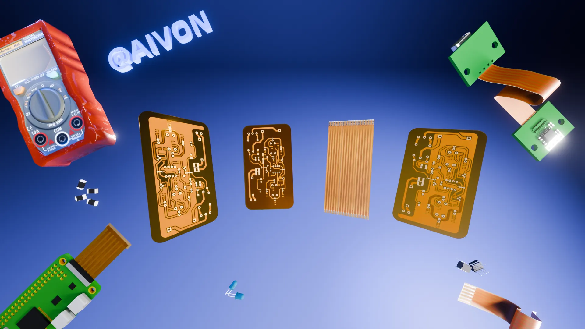
This video explains the fastest way to waste money on your first PCB: treating it like your final production board. Many engineers immediately specify advanced features such as HDI designs, via-in-pad, ENIG finish, and tight design rules before validating core functionality.
The result? When requirements, components, or layouts inevitably change, even small adjustments trigger expensive full re-spins and extended timelines. Instead, the video advocates treating your initial board as a validation tool. Use simpler FR4 PCB stackups, fab-friendly rules, and standard processes that allow you to fail fast, learn quickly, and iterate affordably.
This approach is especially valuable for PCB prototype projects in fast-moving sectors like IoT devices, medical devices, and automotive electronics, where early validation reduces risk and overall development costs. The video provides practical guidance on balancing design ambition with manufacturing reality — helping engineering teams make better decisions before committing to complex multilayer, rigid-flex, or high-frequency builds.
Key Highlights
Don’t Over-Engineer Your First Board: Avoid jumping to HDI, via-in-pad, and tight tolerances before validating your design — this is the fastest route to expensive re-spins.
Treat Prototypes as Learning Tools: Use simple layer stack-up and manufacturer-friendly rules to fail fast, iterate cheaply, and reduce overall project costs.
Validate Early, Optimize Later: Focus first on functionality and basic reliability, then scale to advanced features once requirements are proven.
FAQ
Q1: Why is using HDI or via-in-pad on a first PCB usually a costly mistake?
A1: These advanced features significantly increase fabrication cost and complexity. Until your design is functionally validated, changes become very expensive, often requiring full re-spins instead of simple revisions.
Q2: What’s the best approach for designing a cost-effective first PCB prototype?
A2: Use standard FR4 material, simple stackups, relaxed design rules, and basic finishes like HASL. This allows quick, affordable iterations while you validate functionality before moving to complex features.
Q3: When should you start using advanced PCB technologies like HDI or ENIG?
A3: Only after your initial prototypes have proven the core concept, component selection, and basic layout. Advanced features should be introduced once requirements are stable and risk is minimized.
The fastest way to waste money on your first PCB is designing it like your final product.
I see this all the time.
First board, but you already choose HDI, via-in-pad, ENIG, tight rules everywhere — because it looks professional.
But here's the problem:
nothing has been validated yet.
Your requirements will change.
Your layout will change.
Even your components might change.
And when that happens,
every small mistake forces a full re-spin.
That's how costs explode.
The right mindset is simple:
your first PCB is not a product — it's a validation tool.
Use a simple stackup.Use fab-friendly rules.
Design it to fail fast and learn cheap.
This is AIVON.
Check this before your next layout.