Introduction
Eight-layer printed circuit boards enable complex routing for advanced electronics. These multilayer designs support high-density applications in computing and telecommunications. Understanding 8-layer PCB manufacturing cost helps teams budget effectively. Factors like materials and processes influence total expenses. AIVON assists clients in navigating these elements for optimal value. This article breaks down key cost drivers. It covers 8-layer PCB material cost, fabrication expenses, and assembly charges. Insights guide toward cost-effective 8-layer PCB design strategies. Procurement professionals benefit from clear factor analysis. Designers learn to balance performance with affordability. Explore how choices impact pricing in production runs. AIVON's expertise ensures informed decisions for your projects.
What Is 8-Layer PCB Cost Breakdown and Why It Matters
8-layer PCB cost breakdown examines expenses across design, production, and assembly stages. It includes raw materials, processing, and labor. This multilayer configuration routes signals on eight conductive layers separated by dielectrics. Standards like IPC-6012E qualify these boards for rigid multilayer use.
Cost breakdown matters for project viability. High-density boards serve data centers and medical devices. Unmanaged expenses delay timelines and strain budgets. In procurement, detailed analysis supports supplier negotiations. Assembly teams avoid surprises from overlooked fees.
AIVON observes that early cost reviews reduce overruns. Compliance with IPC-2221B in design minimizes rework charges. Teams achieve reliable boards without excess spending. This approach aligns with quality class requirements in IPC-A-600K.
Factors Influencing 8-Layer PCB Manufacturing Cost
Manufacturing cost for 8-layer PCBs arises from multiple interconnected elements. Layer count increases complexity, raising overall pricing. Base factors include materials, fabrication steps, and scale.
8-Layer PCB Material Cost Drivers
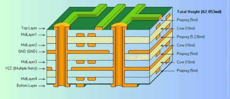
8-layer PCB material cost forms a significant portion of totals. Laminates provide core structure with copper foils and resins. FR-4 grades per IPC-4101E offer standard dielectric properties. Thicker stacks demand more prepreg sheets for interlayer bonding.
Copper weight affects pricing. Heavier foils enhance current handling but add weight and cost. Dielectric thickness influences signal integrity and expense. Specialty materials like high-Tg variants suit thermal demands at premium rates.
Volume impacts material efficiency. Bulk orders lower per-unit costs through economies. AIVON recommends verifying specs against IPC standards to avoid mismatches.
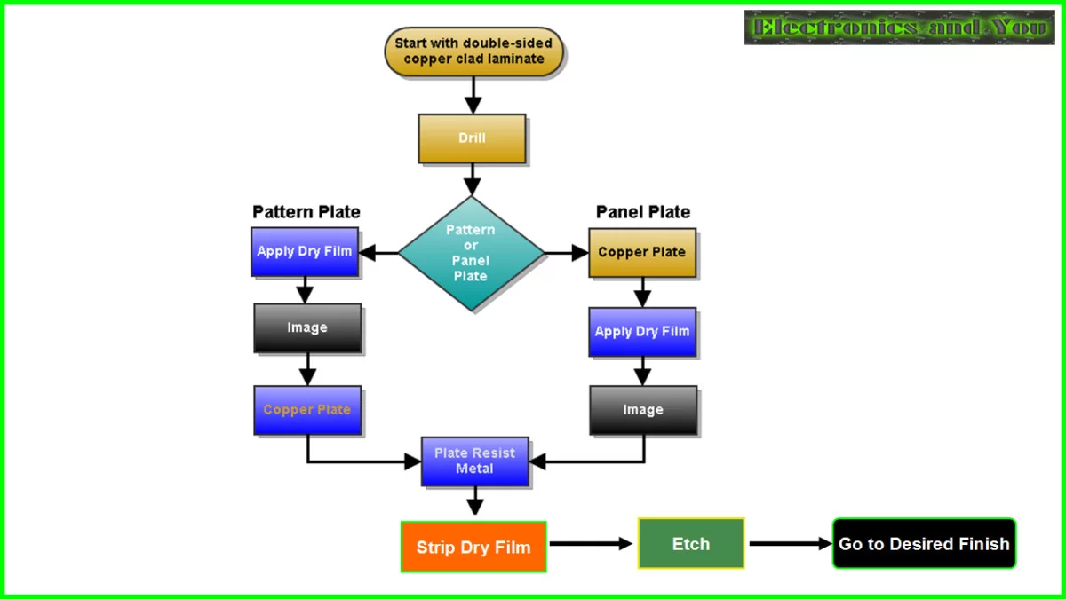
8-Layer PCB Fabrication Cost Components
8-layer PCB fabrication cost covers lamination, drilling, and plating processes. Multilayer pressing aligns cores under heat and pressure. IPC-TM-650 2.4.23 tests bond strength post-lamination.
Drilling creates vias for interlayer connections. Laser methods handle microvias in dense designs. Plating deposits copper in holes, with electrolytic baths ensuring uniformity per IPC-6012E.
Imaging and etching define traces. Multiple exposures per layer extend times. Routing depanel boards, with tabbed edges adding labor. Surface finishes like ENIG protect pads but raise fees over HASL.
Setup charges apply for prototypes. Production runs amortize these over quantities. AIVON streamlines fabrication for consistent quality.
8-Layer PCB Assembly Cost Elements
8-layer PCB assembly cost involves component placement and soldering. Surface mount technology dominates for density. Pick-and-place machines handle fine-pitch parts, with fees based on part count.
Reflow ovens join components via solder paste. Wave soldering suits through-hole elements. Inspection uses automated optical systems per IPC-A-610 for defect detection.
Testing verifies functionality. In-circuit checks probe nets for continuity. Functional tests simulate operation. Rework addresses faults, adding charges for skilled labor.
Turnaround times influence costs. Expedited services incur premiums. AIVON integrates assembly planning to control expenses.
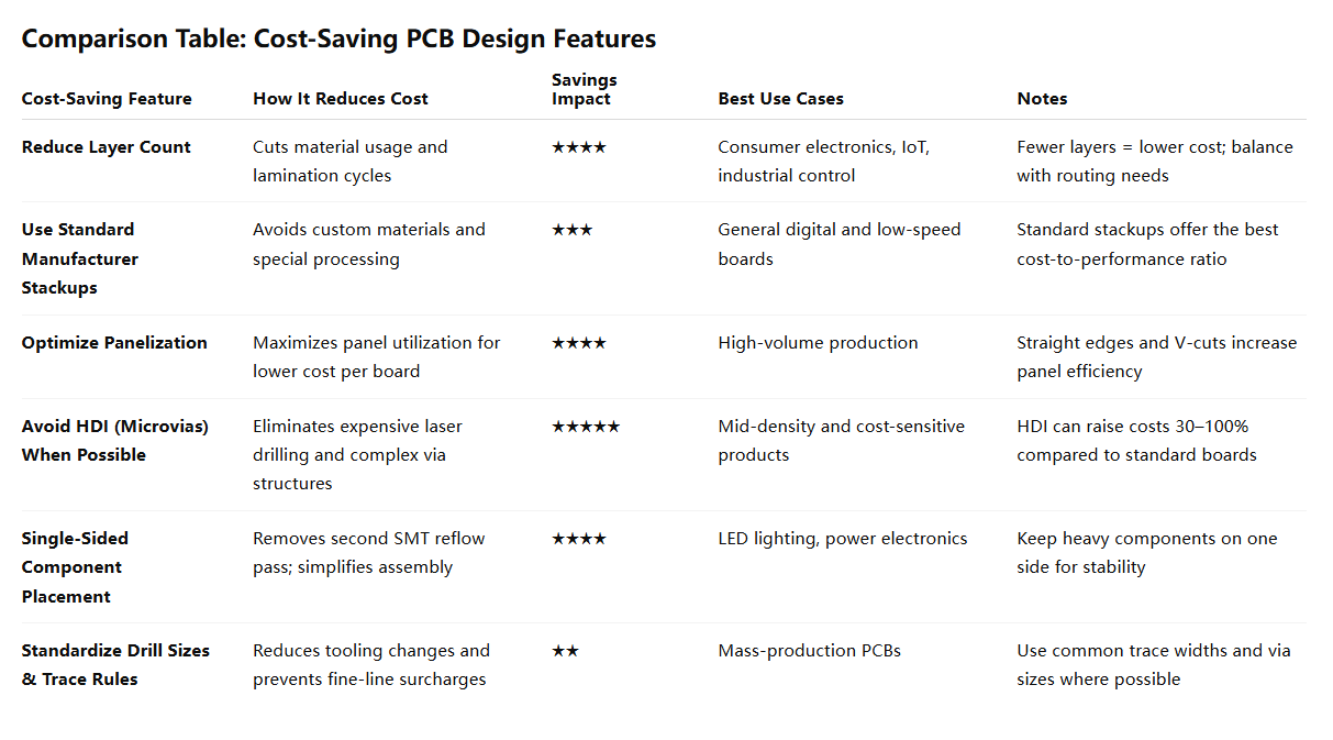
Practical Solutions for Cost-Effective 8-Layer PCB Design
Cost-effective 8-layer PCB design optimizes factors without sacrificing performance. Start with stackup planning. Balance layers for symmetry per IPC-2221B to ease lamination.
Minimize via counts. Use blind and buried types for efficiency. This reduces drilling and plating needs. Route signals on fewer layers where possible.
Select standard materials. FR-4 meets most needs at lower 8-layer PCB material cost. Reserve exotics for critical sections.
Panelize designs. Multiple boards per panel cut fabrication waste. Ensure nesting fits routing constraints.
For assembly, group similar components. This streamlines pick-and-place sequences. Specify lead-free processes to align with RoHS and cut long-term fees.
Simulate thermal profiles early. Tools predict hotspots, avoiding redesigns. AIVON offers DFM reviews to spot cost traps.
Volume forecasting aids negotiations. Prototype small, scale to production. These steps lower overall 8-layer PCB manufacturing cost.
Insights on Achieving Balanced 8-Layer PCB Pricing
Production insights reveal common pitfalls. Oversized panels inflate material use. Tight tolerances demand advanced tooling, hiking fabrication fees.
Assembly delays from part shortages add holding costs. Early BOM reviews prevent this. Layer misalignment in lamination triggers scrap, per IPC-TM-650 inspections.
AIVON case: A client reduced 8-layer PCB assembly cost by 15% through fiducial marks for alignment. Another optimized copper balance, trimming etching waste.
Sustainability choices like thinner coppers save resources. Track metrics across runs for continuous improvement. These practices ensure value.
Conclusion
8-layer PCB cost breakdown highlights materials, fabrication, and assembly as core drivers. Strategic design choices enable affordability. AIVON supports teams in leveraging these factors for success.
Focus on standards like IPC-6012E for quality. Plan holistically to meet budgets. Contact AIVON for tailored guidance on your multilayer needs.
FAQs
Q1: What drives 8-layer PCB manufacturing cost variations?
A1: 8-layer PCB manufacturing cost varies with layer complexity and volume. More layers increase lamination and drilling time. Bulk orders reduce per-unit fees. Material grades and finishes add premiums. AIVON advises DFM checks to identify savings early in the process.
Q2: How does 8-layer PCB material cost impact overall budgeting?
A2: 8-layer PCB material cost depends on laminate type and copper thickness. Standard FR-4 keeps expenses low for general use. High-performance options raise prices for thermal needs. Select based on specs per IPC-4101E. Balance with design requirements for efficient budgeting.
Q3: What factors contribute to 8-layer PCB fabrication cost?
A3: 8-layer PCB fabrication cost includes pressing, plating, and etching steps. Vias and trace densities extend processing. Tolerances and panel sizes influence fees. Follow IPC-6012E for qualification to avoid rework. Streamline routing to minimize these elements.
Q4: How to achieve cost-effective 8-layer PCB design?
A4: Cost-effective 8-layer PCB design uses symmetric stackups and standard vias. Panelization cuts waste. Simulate early to prevent changes. AIVON recommends IPC-2221B compliance for balanced performance. These methods lower total expenses without quality loss.
IPC-6012E — Qualification and Performance Specification for Rigid Printed Boards. IPC, 2017.
IPC-A-600K — Acceptability of Printed Boards. IPC, 2020.
IPC-2221B — Generic Standard on Printed Board Design. IPC, 2009.
IPC-4101E — Specification for Base Materials for Rigid and Multilayer Printed Boards. IPC, 2010.
IPC-TM-650 — Test Methods Manual. IPC, various revisions.
IPC-A-610F — Acceptability of Electronic Assemblies. IPC, 2017.