Why Design Custom PCBs for Your Smart Home?
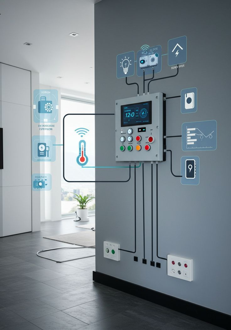
Creating a personalized smart home experience often goes beyond what off-the-shelf devices can offer. Building your own custom Printed Circuit Boards (PCBs) for home automation provides unparalleled flexibility to tailor solutions precisely to your needs, whether it's for advanced lighting control, a sophisticated security system, or an integrated temperature monitoring network. This approach gives you complete authority over features, cost, and crucial security aspects, moving past the limitations and potential expenses of commercial products.
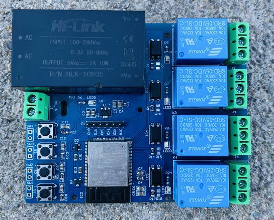
Custom PCBs also enable the consolidation of multiple functionalities onto a single board. Imagine a single unit managing Wi-Fi connectivity, switching high-power appliances via relays, and processing data from various sensors—all while reducing clutter and enhancing overall system reliability. Engaging in these DIY projects not only results in significant cost savings but also offers an invaluable opportunity to develop expertise in electronics design and practical engineering.
Starting Your Custom Smart Home PCB Project: A Step-by-Step Approach
Embarking on a DIY smart home PCB project can seem a bit overwhelming initially, but a structured approach makes it manageable for enthusiasts and seasoned engineers alike. The journey begins with clearly defining your objectives and selecting the right components.
Defining Your Automation Goals
First, pinpoint exactly what you intend to automate. Popular projects often include sophisticated lighting control, real-time monitoring of door and window sensors, or precision management of heating, ventilation, and air conditioning (HVAC) systems. Clearly articulating your goals will guide subsequent design decisions and component choices.
Selecting Key Components and Planning Your Circuit
Next, choose the electronic components essential for your project. Microcontrollers such as the ESP32 or ESP8266 are excellent choices for their integrated Wi-Fi and Bluetooth capabilities. For controlling higher-power devices, relays are indispensable, while various sensors—like temperature sensors, which typically operate within a range of -40°C to 125°C—provide necessary data input. Before committing to a layout, sketch a basic circuit diagram to visualize component interconnections, a critical step that helps preempt costly design errors.
Selecting the Ideal Software for Home Automation PCB Design
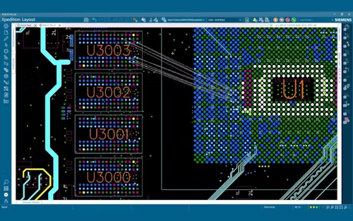
Precision is paramount in PCB design, necessitating software that offers robust schematic and layout capabilities. For home automation projects, the ideal PCB design software balances user-friendliness with advanced features capable of handling complex circuits.
Essential Software Features
Look for tools equipped with a powerful schematic editor, allowing you to draw and simulate your circuit before any physical construction. Robust PCB layout tools are essential for accurately arranging components and routing traces, minimizing potential issues like signal interference. Extensive component libraries—providing access to a wide array of parts such as resistors, capacitors, and microcontrollers—are also crucial. Furthermore, simulation capabilities that can test parameters like impedance (typically 50-100 ohms for most traces) and signal integrity are invaluable for pre-manufacturing validation.
Many advanced software packages also facilitate direct integration with manufacturing services, streamlining the process of ordering your custom boards. If you're new to PCB design, prioritize software that offers comprehensive tutorials and strong community support to ease the learning curve.
Leveraging Open Source Resources for PCB Schematics
For those who prefer not to start a PCB design from scratch, open-source home automation PCB schematics offer an excellent alternative. These designs are freely shared by the broader maker community and can be adapted to fit specific project requirements, providing a significant head start.
Benefits of Open Source Schematics
● Accelerated Development: Utilize pre-engineered schematics for common applications like relay control boards or sensor hubs, drastically cutting down design time.
● Educational Value: Gain insights into best practices by examining how experienced designers approach trace routing and component placement to mitigate issues such as crosstalk or thermal buildup.
● Cost Efficiency: Avoid the expense associated with professional design services by customizing existing, validated designs.
You can find a wealth of open-source schematics on platforms like GitHub or specialized electronics forums. Always thoroughly review these designs for any potential errors and confirm their compatibility with your chosen components, paying close attention to specifications like voltage ratings (e.g., 3.3V or 5V for microcontrollers).
Building a Wireless Home Automation PCB
Wireless connectivity is foundational to modern smart home systems. Developing a custom wireless home automation PCB unlocks vast possibilities for controlling devices remotely and integrating with intelligent assistants.
Key Steps for Wireless PCB Design
1. Module Selection: Opt for a versatile wireless module, such as the ESP32, which natively supports both Wi-Fi and Bluetooth, typically operating at a frequency of 2.4 GHz.
2. Antenna Layout: Design the antenna layout meticulously, ensuring precise trace length and impedance matching (often around 50 ohms) to prevent signal degradation.
3. Power Management: Incorporate stable voltage regulators to deliver a consistent 3.3V supply to the wireless module, as voltage fluctuations can severely disrupt connectivity.
4. Post-Assembly Testing: After assembly, rigorously test the board's operational range and signal strength using tools like a spectrum analyzer, aiming for a reliable signal strength exceeding -70 dBm.
Wireless PCBs are ideal for smartphone app control or voice assistant integration. Remember, effective shielding is crucial to protect against interference from other electronic devices within the home environment.
Troubleshooting Common Issues in Home Automation PCBs
Even with meticulous planning, issues can emerge during or after PCB construction. Mastering home automation PCB troubleshooting is vital to ensure your projects operate as intended.
Addressing Common PCB Problems
● Power Failure: Investigate for broken traces or "cold" solder joints. Utilize a multimeter to confirm continuity and verify that the intended input voltage (e.g., 5V or 12V) reaches all components.
● Signal Interference: If your wireless module experiences connectivity issues, inspect for crosstalk between traces. Re-route high-frequency signals away from power supply lines.
● Overheating: Excessive heat (exceeding 85°C for most ICs) can damage components. Implement passive cooling solutions like heat sinks or actively improve airflow within your design.
● Firmware Glitches: If the board powers on but fails to function, debug the microcontroller's firmware. Employ serial monitoring to pinpoint and rectify coding errors.
Troubleshooting demands patience, but maintaining a detailed log of each diagnostic step can help identify patterns and prevent recurrence. Always test individual sections of your board before full assembly to catch problems early.
Designing a Stable Power Supply for Home Automation PCBs
A robust power supply forms the essential foundation of any reliable smart home system. Therefore, home automation PCB power supply design requires focused attention, as inadequate power management can lead to system instability or component damage.
Principles for Stable Power Design
● Voltage Regulation: Implement linear or switching regulators to efficiently step down the input voltage (e.g., from 12V to 5V) for sensitive microcontrollers and sensors.
● Current Capacity: Verify that your power supply can adequately support the total current draw of all components. For instance, a relay switching a 10A load necessitates a high-capacity supply and sufficiently thick traces (at least 1mm wide for high-current paths).
● Noise Reduction: Integrate decoupling capacitors (typically 0.1μF placed close to ICs) to effectively filter out electrical noise and maintain voltage stability.
● Backup Power: For critical systems like security sensors, consider incorporating a small battery backup, such as a 3.7V LiPo cell.
Thoroughly testing your power supply under maximum load conditions is essential. Use a multimeter to check for any significant voltage drops (ideally less than 0.2V) across critical points on your board.
Securing Your Smart Home with Robust PCB Design
Given that smart home devices are frequently internet-connected, security becomes a paramount concern. Secure home automation PCB design encompasses both hardware and software strategies to defend against potential cyber threats.
Implementing Security Measures
● Encrypted Communication: Utilize microcontrollers with integrated encryption capabilities for Wi-Fi data transmission, ensuring that signals cannot be easily intercepted.
● Physical Protection: Employ tamper-resistant enclosures to deter unauthorized physical access to your HDI PCB.
● Firmware Integrity: Implement secure boot mechanisms and commit to regular firmware updates to patch newly discovered vulnerabilities in your code.
● Power Isolation: Use optocouplers to electrically separate high-voltage sections (like relay outputs) from low-voltage control circuits, thereby minimizing the risk of electrical faults affecting sensitive components.
Security is an ongoing commitment. Continuously monitor your network for suspicious activity and maintain backups of your firmware to facilitate rapid recovery in the event of a security breach.
Bringing Your Vision to Life: PCB Manufacturing
Once your design is finalized and thoroughly vetted, the next exciting step is manufacturing your fast turn custom PCB. Collaborating with a reputable fabrication service is crucial to ensure the production of high-quality boards.
Key Considerations for Manufacturing
● Design Files: Export your schematic and layout files into a widely accepted industry standard format, such as Gerber, for manufacturing.
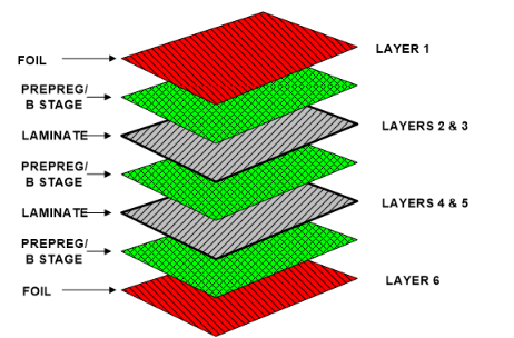
● Material Selection: For most home automation PCBs, FR4 material is an excellent choice due to its balance of durability and cost-effectiveness.
● Layer Count: For simpler projects, single or double-layer boards are typically sufficient and help keep production costs down.
● Prototyping: Always order a small batch initially to thoroughly test functionality before committing to full-scale production.
Manufacturing your PCB is the culmination of your design efforts, transforming your innovative ideas into tangible hardware. Platforms like AIVON can significantly streamline this process, from initial design submission to final delivery, ensuring your smart home automation project moves from concept to reality efficiently.
Conclusion: Empowering Your Home with Custom Automation
Designing and building custom PCBs for smart home automation offers a uniquely satisfying and practical method to enhance your living environment. By dedicating yourself to DIY home automation PCB projects, skillfully utilizing appropriate home automation PCB design software, and exploring the wealth of open-source home automation PCB schematics, you gain the ability to craft solutions perfectly aligned with your specific needs.
Equally important are the practices of effective home automation PCB troubleshooting, robust home automation PCB power supply design, and meticulous secure home automation PCB design—all crucial for ensuring the reliability and safety of your system. With the comprehensive guidance provided in this article, you are well-equipped to begin powering up your home with bespoke electronics. Start with manageable projects, test frequently, and immerse yourself in the rewarding process of transforming your smart home aspirations into functional realities.