PCB Specifications
| Parameter | Value | Parameter | Value |
|---|---|---|---|
| PCB Type | FR4 PCB | Quantity | 5 pcs |
| Layers | 4 Layers | Board Type | Panel PCB |
| Dimensions | 135 x 225 mm | Copper Weight | 1oz |
| Thickness | 1 mm | Min Track / Spacing | 6/6mil↑ |
| Surface Finish | ENIG (Immersion Gold) | Min Hole Size | 0.2mm |
| Solder Mask | Green | Silkscreen | White |
| Stack-up | Custom | Impedance Control | Yes |
Manufacturing Timeline
Logistics Information
Key Manufacturing Processes
Manufacturing Summary
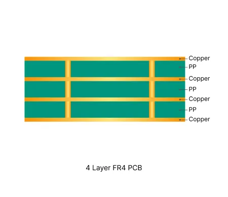
This production record documents the manufacturing of a standard 4-layer FR4 PCB featuring impedance control and immersion gold ENIG surface finish. The board utilized a 1.6 mm finished thickness with 1 oz copper on all layers. Minimum track width and spacing stood at 5/5 mil, placing the geometry in the tighter range that requires precise process controls. Engineering review included stackup impedance engineering and trace width compensation to meet the specified electrical requirements.
High pressure lamination followed inner layer imaging and circuit etching, with special attention to layer stack alignment for optimal registration. Solder mask was applied prior to the electroless nickel deposition and immersion gold deposition steps. Post-production, TDR impedance testing validated the controlled impedance values across multiple traces, and comprehensive electrical testing ensured no opens or shorts in the final product.
Completed over 3.5 days, the order was executed with attention to each critical step, resulting in boards that meet both dimensional and performance criteria consistently. This reflects the actual manufacturing sequence used to deliver reliable impedance controlled PCBs.
Explore More PCB Manufacturing Resources

Real Production Records
| Order ID | PCB Type | Layers | Dimensions | Solder Mask | Surface Finish | Quantity | Action |
|---|---|---|---|---|---|---|---|
| FR4-20260520-046 | FR4 PCB | 2 | 94.21 x 275 | Green | ENIG (Immersion Gold) | 75 | View detail |
| FR4-20260515-068 | FR4 PCB | 14 | 244 x 267 | Green | ENIG (Immersion Gold) | 10 | View detail |
| FR4-20260512-016 | FR4 PCB | 4 | 63.5 x 127 | Green | ENIG (Immersion Gold) | 10 | View detail |


