










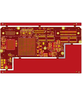
PCB Specifications
| Parameter | Value | Parameter | Value |
|---|---|---|---|
| PCB Type | FR4 PCB | Quantity | 5 pcs |
| Layers | 18 Layers | Board Type | Panel PCB |
| Dimensions | 163 x 102 mm | Copper Weight | 1oz |
| Thickness | 2 mm | Min Track / Spacing | 3/3mil |
| Surface Finish | ENIG (Immersion Gold) | Min Hole Size | 0.1mm |
| Solder Mask | Red | Silkscreen | White |
| Stack-up | Custom | Impedance Control | Yes |
Manufacturing Timeline
Logistics Information
Key Manufacturing Processes
Manufacturing Summary
This 18-layer FR-4 PCB (163 × 102 mm, 2.0 mm finished thickness, TG170 S1000-2M material) was produced as a 5-piece urgent batch with 0.1 mm minimum hole size and 3 mil minimum line/space. Outer copper started at 0.5 oz base with 1 oz target after plating, while inner layers used standard 0.5 oz. The design required full impedance control, ENIG surface finish, resin plugging, and press-fit hole preparation. Production followed 100% flying probe testing and mechanical forming, with a 50-day delivery window from order confirmation.
During CAM engineering review, several stackup-related conflicts emerged. L2 and L15 copper thickness assumptions for 1 oz finished would have caused most impedance values to fall out of specification, while designated 11.5 mil reference lines on L2 were shielded by L3, preventing direct measurement. Additional issues included unclear press-fit hole diameters not detailed in the fabrication notes or drill drawings, conflicting copper plating calls on L11 (no blind vias present), and partial shielding of impedance traces across reference layers that would introduce deviation. Material thermal conductivity requirements (1.0 W/m·K) also conflicted with standard FR-4 values. We adjusted the stackup configuration and fine-tuned specific impedance line widths to achieve target values, confirming all changes with the customer before proceeding. 18-layer FR-4 impedance compensation followed established internal guidelines for reference layer shielding and copper distribution control.
All engineering changes were documented and approved prior to inner layer imaging. Resin plugging, plating (minimum 30 μm hole copper), and solder mask application completed without deviation. Final electrical testing confirmed impedance compliance within tolerance, and the boards were delivered on schedule with full test reports and quality certificates. This production record demonstrates reliable execution of high-layer count, impedance-controlled boards with tight geometry features under standard FR-4 constraints.
Explore More PCB Manufacturing Resources
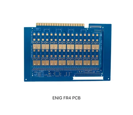
ENIG FR4 PCB Manufacturing Insights
FR4 material with ENIG finish provides balanced electrical performance, shelf life, and assembly compatibility for industrial and high-reliability electronics.
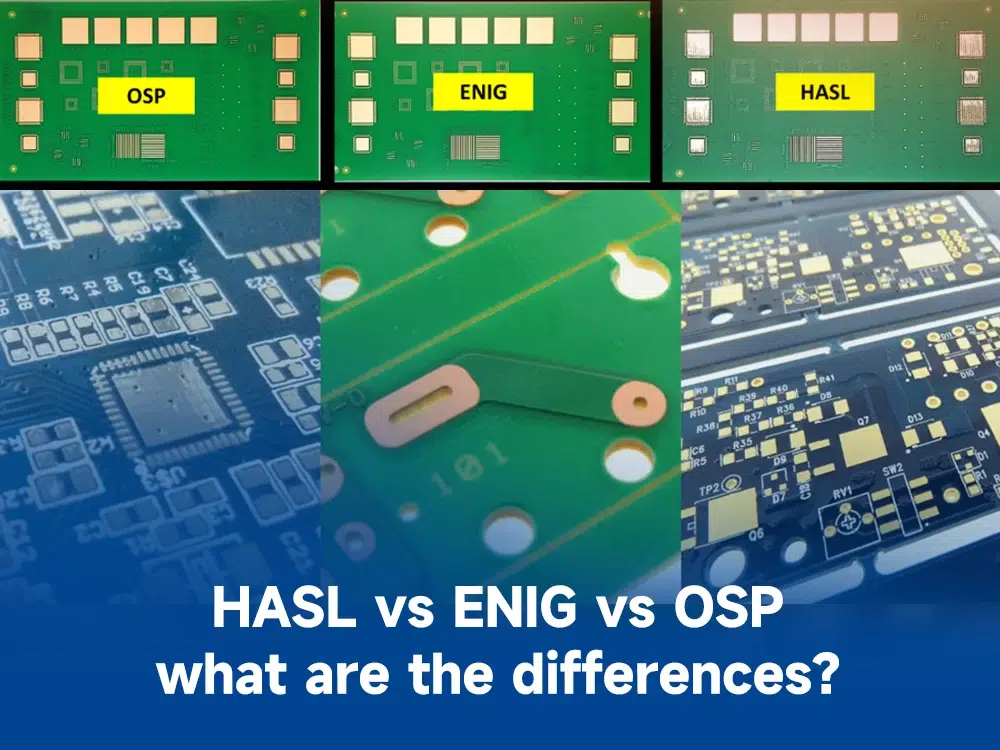
FR4 PCB Surface Finish Guide: ENIG vs HASL vs OSP DFM Issues and Engineering Queries
Explore common engineering queries in ENIG, HASL, and OSP FR4 PCBs. Learn real DFM challenges, surface finish compatibility issues, and practical solutions to reduce manufacturing risks and improve yield.
Real Production Records
| Order ID | PCB Type | Layers | Dimensions | Solder Mask | Surface Finish | Quantity | Action |
|---|---|---|---|---|---|---|---|
| FR4-20260819-043 | FR4 PCB | 10 | 157 x 140 | Blue | ENIG (Immersion Gold) | 100 | View detail |
| FR4-20260818-014 | FR4 PCB | 2 | 110.32 x 173.3 | Green | ENIG (Immersion Gold) | 200 | View detail |
| FR4-20260811-033 | FR4 PCB | 8 | 226.8 x 10⁹ | Green | ENIG (Immersion Gold) | 50 | View detail |


