










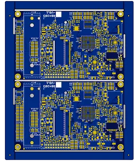
PCB Specifications
| Parameter | Value | Parameter | Value |
|---|---|---|---|
| PCB Type | FR4 PCB | Quantity | 10 pcs |
| Layers | 8 Layers | Board Type | Panel PCB |
| Dimensions | 130 x 161.6 mm | Copper Weight | 1oz |
| Thickness | 1.6 mm | Min Track / Spacing | 4/4mil |
| Surface Finish | ENIG (Immersion Gold) | Min Hole Size | 0.15mm |
| Solder Mask | Blue | Silkscreen | White |
| Stack-up | Custom | Impedance Control | No |
Manufacturing Timeline
Logistics Information
Key Manufacturing Processes
Manufacturing Summary
This 8-layer board used KB-6165F TG150 material at 1.6 mm thickness with 0.5 oz inner and 1 oz outer copper. Measuring 130 × 161.6 mm, the design incorporated blind vias at 0.15 mm laser diameter, 4 mil minimum trace and space, ENIG finish, blue solder mask, and V-cut plus routing separation on a 1×2 panel. Twenty pieces were produced under a 21-day schedule after customer self-panelization.
CAM review flagged oversized solder mask openings that eliminated bridges between pads and exposed traces, via capping conflicts on double-sided open holes without tin, non-standard 0.15 mm laser vias, BGA pads requiring non-solder-mask-defined treatment to prevent cratering, and legend frames too close to pads. Additional items included V-cut copper clearance of 0.45 mm per side, process-edge test pads on all four sides, and confirmation of the KB TG150 stack-up. Openings were reduced to restore mask bridges, via plugging requirements were clarified on the production files, BGA pads were redefined, legend positions were adjusted, and V-cut test features were added to the edges.
All changes were incorporated before release. One-hundred-percent flying-probe testing was completed, and boards shipped with electrical test reports and quality certificates. The revisions addressed the blind via and solder mask constraints while preserving the specified V-cut process.
Explore More PCB Manufacturing Resources
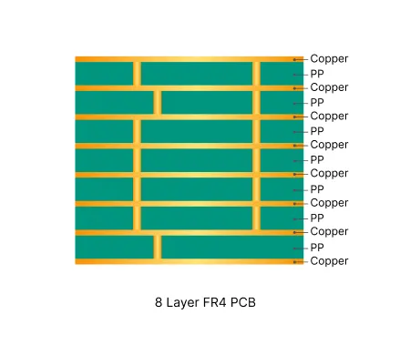
8 Layer FR4 PCB Manufacturing Insights
These boards integrate multiple microvia layers to support complex routing and high signal density in advanced electronics.

Multilayer FR4 PCB Engineering Queries Explained: Causes, Risks and Solutions
In-depth guide to the most frequent Engineering Queries (EQ) and DFM issues in Multilayer FR4 PCB (4/6/8+ layers) production. Real factory insights on stack-up confirmation, impedance control, copper balance, inner layer design, via treatment, registration, and practical prevention strategies.
Real Production Records
| Order ID | PCB Type | Layers | Dimensions | Solder Mask | Surface Finish | Quantity | Action |
|---|---|---|---|---|---|---|---|
| FR4-20260918-033 | FR4 PCB | 6 | 55 x 41.7 | Green | ENIG (Immersion Gold) | 5 | View detail |
| FR4-20260912-059 | FR4 PCB | 2 | 275 x 193.7 | Green | ENIG (Immersion Gold) | 100 | View detail |
| FR4-20260819-043 | FR4 PCB | 10 | 157 x 140 | Blue | ENIG (Immersion Gold) | 100 | View detail |


