Why Is Thoughtful Router PCB Design Essential?
Router printed circuit boards (PCBs) form the foundational hardware for all networking devices, orchestrating the flow of data across networks. A meticulously designed PCB is paramount for ensuring consistent performance, minimizing unwanted signal interference, and effectively managing power consumption. For those new to electronics design, grasping the specific complexities of router PCBs—such as routing high-speed signals, achieving correct impedance matching, and managing heat dissipation—is critically important.
Neglecting these design considerations can lead to significant issues, including frequent connection drops, sluggish data transfer speeds, or even outright hardware malfunctions. This guide aims to equip hobbyists, students, and new engineers with the core principles needed to design a functional router board. By adhering to these steps, you can create a PCB capable of meeting fundamental networking demands while sidestepping common design pitfalls.

What Are the Initial Steps in Router PCB Design?
Embarking on a router PCB design project requires a structured approach, beginning with a solid understanding of the fundamental elements involved. A typical router PCB incorporates a microprocessor or microcontroller for data processing, Ethernet controllers for network connectivity, dedicated power management circuitry, and various connectors for external interfaces. The board layout must be capable of accommodating high-speed signals, which often range from 100 MHz to several gigahertz, depending on the router's performance capabilities.
Setting Realistic Project Goals
For beginners, it’s advisable to start with a straightforward design objective, such as a basic single-band Wi-Fi router for simple internet routing tasks. This approach simplifies the learning curve, allowing you to focus on critical concepts like signal integrity and efficient power distribution without being overwhelmed. A good rule of thumb is to aim for a design that supports data rates of at least 100 Mbps for an entry-level router, a target that is achievable using readily available components and standard PCB mass production process.
Unique Aspects of Router PCB Layouts
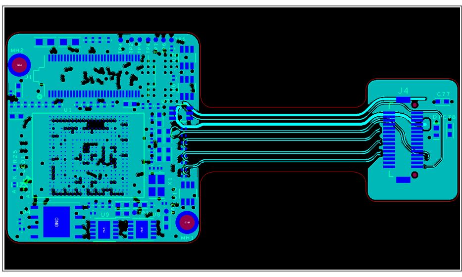
Unlike general-purpose PCBs, router designs place a strong emphasis on optimizing high-speed signal pathways and ensuring robust electromagnetic compatibility (EMC). Signals must travel cleanly without interference, necessitating careful trace routing to prevent crosstalk between adjacent lines. Furthermore, routers frequently require multilayer boards (typically four layers or more) to effectively isolate power, ground, and various signal planes, which is crucial for maintaining pristine operational performance.
How Do You Define Requirements and Select Components for a Router PCB?
Every successful PCB design starts with a clear articulation of its intended functionality and performance targets. Before diving into component selection, it’s essential to outline what your router needs to accomplish.
Defining Your Router’s Specifications
Consider whether your router will support only wired connections or if it will include Wi-Fi capabilities. What specific data speeds are you aiming for? For an initial project, these specifications are a good starting point:
● Data Speed: Begin with 100 Mbps (Fast Ethernet).
● Ports: Include one WAN port and 2-4 LAN ports.
● Power: Plan for a 5V or 12V input, with a current rating of 1-2A.
● Wi-Fi (Optional): If included, consider a single-band 2.4 GHz module.
Documenting these requirements will serve as a critical guide for both component selection and the subsequent schematic design, helping to prevent scope creep and keep your project manageable.
Essential Component Choices for Router PCBs
Selecting the appropriate components is a pivotal step. For beginners, it's wise to focus on parts that are widely available, thoroughly documented, and supported by a strong community. Here’s a breakdown of key components:
● Microcontroller or SoC: This acts as the router’s central processing unit, handling data traffic. For a basic design, choose a chip with integrated Ethernet support and adequate processing power (e.g., 100-300 MHz clock speed). Leveraging development boards or reference designs can significantly simplify integration.
● Ethernet Controllers and PHYs: These manage the wired network connections. For simplicity, opt for components that support 10/100 Mbps. Ensure the Physical Layer Device (PHY) is compatible with your microcontroller’s interface, commonly SPI or MII.
● Power Management ICs: Routers demand stable power delivery, often requiring voltage regulators to step down the input voltage (e.g., 12V to 3.3V or 1.8V for digital circuits). Select regulators with an output capacity of at least 1.5A to accommodate peak loads.
● Connectors and Passive Components: Standard RJ45 connectors are necessary for Ethernet ports. Verify that capacitors and resistors meet the voltage and current ratings of your design. For high-speed signals, employ low ESR (Equivalent Series Resistance) decoupling capacitors, typically 0.1 μF, placed near IC pins. Always consult component datasheets for pin compatibility and power requirements, as mismatches can lead to design failures.
How to Design the Schematic and Choose PCB Software?
After selecting components, the next phase involves creating the schematic—a detailed electrical blueprint of how all parts interconnect. This step is crucial for validating the electrical correctness of your design before proceeding to the physical layout.

Best Practices for Schematic Design
● Functional Organization: Group components into logical blocks (e.g., power, processor, Ethernet) to enhance clarity.
● Reference Designs: Many chip manufacturers provide sample schematics; adapt these to fit your project’s specific needs.
● Decoupling Capacitors: Strategically place 0.1 μF capacitors near the power pins of integrated circuits to suppress noise.
● Net Labeling: Clearly name all connections (e.g., “VCC_3.3V”) to minimize errors during the layout stage.
For a router, ensure that high-speed signal paths, such as Ethernet lines, are explicitly marked for future differential pair routing. A typical Ethernet connection requires impedance matching, often 100 ohms for differential pairs, which should be clearly noted in your schematic.
Selecting the Right PCB Design Software
Your PCB design software is the primary tool for translating your schematic into a physical layout. For beginners, choose software that offers a balance between user-friendliness and essential features, including multilayer support and robust design rule checks (DRC).
● Key Software Features: Look for a comprehensive schematic editor, a capable layout editor, integrated DRC to identify errors like incorrect trace widths or spacing, extensive library support for component footprints and symbols, and the ability to export industry-standard Gerber files for manufacturing.
Many software options provide free versions suitable for hobbyists or students, offering sufficient functionality for a basic router design. Dedicate time to learning the software through tutorials to streamline your project timeline.
What Are the Fundamentals of Router PCB Layout?
With a completed schematic, the next critical step is to design the PCB layout, which involves physically arranging components and routing traces on the board. For router PCBs, the layout directly influences performance due to the presence of high-speed signals and significant power demands.
Essential Layout Principles for Beginners
● Multilayer Boards: Routers commonly utilize 4-layer boards, dedicating layers for signals, ground, power, and additional signals. This stratification significantly aids in noise reduction.
● Logical Component Placement: Position high-speed components, such as Ethernet PHYs, as close as possible to their respective connectors to minimize trace lengths.
● Differential Pair Routing: Ethernet signals often rely on differential pairs. It's crucial to maintain equal length and consistent spacing (typically 5-10 mils apart) to ensure a 100-ohm impedance.
● Dedicated Ground Plane: Allocate an entire layer for ground to effectively reduce noise. Connect all ground pins directly to this plane using vias.
● Appropriate Trace Widths: Use wider traces for power lines (e.g., 20-30 mils for 1A current) and narrower traces for signal lines (e.g., 6-10 mils).
For an entry-level router design, aim for a board size of approximately 100mm x 100mm to control manufacturing costs while accommodating essential components. Always use the design rule checks within your software to verify that spacing and widths comply with manufacturing standards (e.g., a minimum 6-mil trace width for most fabricators).
How to Validate, Test, and Manufacture Your Router PCB?
Before committing your design to manufacturing, thorough validation and testing are indispensable steps to ensure functionality and prevent costly errors.
Design Validation and Initial Testing
Execute a comprehensive design rule check (DRC) to identify any issues like unconnected pins or incorrect spacing. If your software permits, simulate high-speed signals to confirm signal integrity. Specifically for Ethernet lines, ensure that the differential pair length mismatch is less than 50 mils to avoid timing problems at 100 Mbps.
Once the PCB is manufactured, begin by testing the bare board with a multimeter to verify continuity and check for any power-related anomalies. Progress to using a basic network testing tool to confirm that data transmission operates as anticipated.
Manufacturing Your Router PCB
Upon finalizing your design, generate Gerber files from your PCB software. These files contain all the necessary layer information for the large PCB manufacturer. It's crucial to double-check these files using a Gerber viewer to ensure no data is missing or corrupted. Select a reputable PCB fabrication service that supports multilayer boards and offers efficient turnaround times for prototyping.
For a beginner’s router PCB, anticipate manufacturing costs ranging from $10 to $20 for a small batch of 2-5 boards, depending on the board size and layer count. It’s always prudent to order a few extra boards for additional testing and to account for any potential manufacturing defects.
What Common Pitfalls Should Beginners Avoid in Router PCB Design?
As a newcomer to PCB design, certain mistakes are frequently encountered. Being aware of these common pitfalls can help you avoid them.
Key Mistakes to Sidestep
● Neglecting Signal Integrity: Prolonged traces or improper routing can severely degrade high-speed signals. Always keep Ethernet traces short and ensure they are length-matched.
● Inadequate Power Distribution: Insufficient decoupling capacitors can lead to detrimental voltage drops. Place these capacitors strategically near every IC power pin.
● Overcomplicating the Design: Begin with a simple project. Attempting to incorporate too many advanced features (e.g., dual-band Wi-Fi) can overwhelm a first-time designer.
● Lack of Ground Planes: Not dedicating a solid ground plane can lead to significant noise issues and signal integrity problems.
Enhancing Your Router PCB Design Skills
Mastering PCB design is an iterative process that benefits greatly from consistent practice. Start with smaller projects before progressing to more complex router designs. Study open-source hardware designs to gain insights into effective layout strategies and component choices. Engage with online forums and communities to learn from seasoned designers and share your progress.
Continuously educate yourself on evolving high-speed design rules, especially as router technology advances. For instance, contemporary routers often require signals up to 5 GHz for Wi-Fi 6, demanding much tighter impedance control (e.g., 50 ohms for RF traces) and the use of specialized board materials.