PCB Specifications
| Parameter | Value | Parameter | Value |
|---|---|---|---|
| PCB Type | FR4 PCB | Quantity | 5 pcs |
| Layers | 20 Layers | Board Type | Panel PCB |
| Dimensions | 270 x 353.8 mm | Copper Weight | 1oz |
| Thickness | 2.5 mm | Min Track / Spacing | 4/4mil |
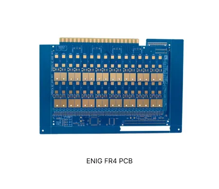
| Surface Finish | ENIG (Immersion Gold) | Min Hole Size | 0.3mm↑ |
| Solder Mask | Red | Silkscreen | White |
| Stack-up | Custom | Impedance Control | Yes |
Manufacturing Timeline
Logistics Information
Key Manufacturing Processes
Manufacturing Summary
This 20-layer FR4 PCB order was completed as a 5-piece run of single boards measuring 270 × 353.8 mm with a final finished thickness of 2.5 mm. The build used TU-863 high-Tg base material, 0.5 oz outer / 1 oz inner copper weights, and full ENIG surface finish. Controlled impedance was a key requirement, with 50 Ω single-ended traces on L1 and both 50 Ω and 100 Ω differential pairs on L18, supported by the verified stack-up report. Extensive via resin plugging was also specified to ensure reliability in high-density areas.
During the engineering DFM review, multiple specification conflicts and process risks were identified and resolved through detailed customer communication. Board thickness notations differed between the main order and remarks, requiring clarification to prevent out-of-tolerance results that could affect assembly fit and mechanical stability. Process edge design initially called for V-cut but was changed to stamp-hole routing; the sharp right-angle corners on these edges posed a risk of damaging packaging during shipment, so edge treatment and copper balancing were added to improve flow and reduce stress. Significant copper density imbalance between layers raised concerns about warpage on this relatively thick multilayer board — excessive bow or twist could lead to soldering defects or reliability issues in final use. Inner-layer non-functional pads on high-speed nets were flagged as they could introduce unnecessary stubs and degrade signal integrity; confirmation was obtained to retain or remove them as needed. Via plugging presented a particular challenge: many vias had solder mask windows 4 mil larger than the hole on both sides, making complete resin fill and subsequent mask coverage difficult and risking ink migration or incomplete plugging that might cause long-term reliability problems. Additional clarifications covered copper foil types (HTE on outer layers, RTF on inner layers), prepreg thickness adjustment (+0.15 mm between L10-L11) to achieve the precise 2.5 mm target, and exact content/placement of date, batch, and SN markings given the absence of UL certification for the specific red solder mask on TU-863 material.
Through iterative engineering discussions, optimized drilling compensation, selective plugging strategy (resin fill only where mask design permitted), adjusted prepreg configuration, and confirmed marking approach on the process edge, all issues were successfully addressed without compromising design intent. The order was manufactured within the 18-day delivery window, underwent 100% flying probe electrical testing, and passed full verification of impedance values, board thickness tolerance, and mechanical dimensions. Final boards demonstrated excellent flatness and plating quality, confirming reliable execution of this high-layer-count, impedance-controlled PCB.
Explore More PCB Manufacturing Resources
Real Production Records
| Order ID | PCB Type | Layers | Dimensions | Solder Mask | Surface Finish | Quantity | Action |
|---|---|---|---|---|---|---|---|
| FR4-20260520-046 | FR4 PCB | 2 | 94.21 x 275 | Green | ENIG (Immersion Gold) | 75 | View detail |
| FR4-20260519-001 | FR4 PCB | 10 | 67.6 x 42 | Green | Gold Plating | 20 | View detail |
| FR4-20260515-068 | FR4 PCB | 14 | 244 x 267 | Green | ENIG (Immersion Gold) | 10 | View detail |


