High Tg FR4 PCB Production Record #FR4-20260519-001
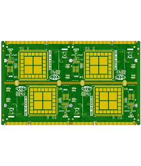
| Parameter | Value | Parameter | Value |
|---|---|---|---|
| PCB Type | FR4 PCB | Quantity | 20 pcs |
| Layers | 10 Layers | Board Type | Panel PCB |
| Dimensions | 67.6 x 42 mm | Copper Weight | 1oz |
| Thickness | 1 mm | Min Track / Spacing | 6/6mil↑ |
| Surface Finish | Gold Plating | Min Hole Size | 0.3mm↑ |
| Solder Mask | Green | Silkscreen | White |
| Stack-up | Custom | Impedance Control | Yes |
This 10-layer FR-4 board (67.6 × 42 mm, 1.0 mm finished thickness, TG170 S1000-2M material) was produced in a 2×2 panel arrangement for a total of 20 pieces. Outer copper was 1 oz with 0.5 oz inner layers, 6/6 mil minimum line/space, 0.3 mm minimum hole size, and full 100% flying probe testing. Key process requirements included impedance control, one-side half-cut holes, V-scoring, green solder mask, white legend, and electroplated gold finish with gold finger beveling. Resin plugging was applied to specified vias per final confirmation.
During DFM review, several engineering questions required resolution. Via plugging confirmation was needed for 32 × 0.2 mm through vias with double-sided opening and six 0.406 mm holes. Gold finger beveling presented edge proximity challenges; our minimum 0.3 ± 0.1 mm bevel depth resulted in approximately 0.25 mm finger edge reduction to avoid copper exposure. Impedance lines specified in documentation were not located in the provided files; we recalculated using actual Gerber trace widths and adjusted target board thickness to 1.13 mm ±10% to achieve required values, with inner layer single-ended lines limited to 46 Ω due to dielectric and geometry constraints.
All engineering questions were confirmed with the customer prior to production release. The order completed within the 23-day delivery window with mechanical forming for the final panels. Electrical testing, quality documentation, and shipment records confirm full compliance with the specified parameters and controlled processes.
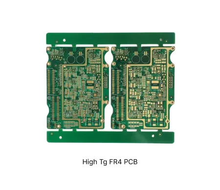
High Tg FR4 delivers improved thermal resistance and dimensional stability for applications requiring sustained performance under thermal stress.
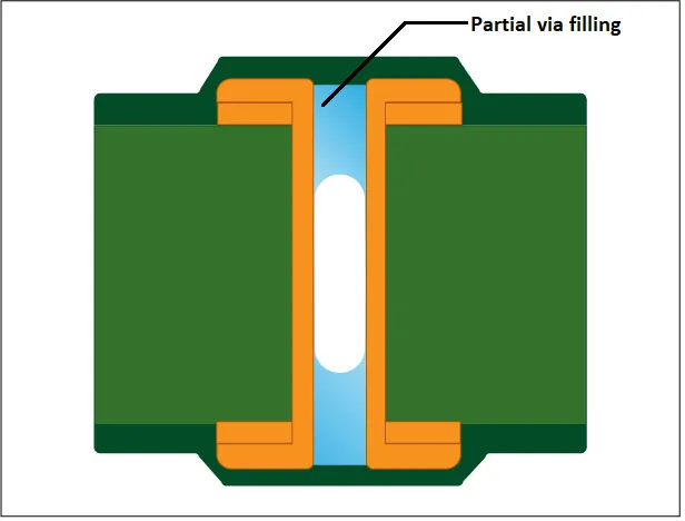
Stop production delays in High Tg FR4 PCB projects. A senior engineer explains common manufacturing queries regarding material stability, thermal stress, and stack-up adjustments for high-reliability boards.
| Order ID | PCB Type | Layers | Dimensions | Solder Mask | Surface Finish | Quantity | Action |
|---|---|---|---|---|---|---|---|
| FR4-20260519-059 | FR4 PCB | 6 | 192.53 x 149.86 | Green | ENIG (Immersion Gold) | 15 | View detail |
| FR4-20260515-068 | FR4 PCB | 14 | 244 x 267 | Green | ENIG (Immersion Gold) | 10 | View detail |
| FR4-20260505-010 | FR4 PCB | 8 | 88.4 x 90.2 | Green | ENIG (Immersion Gold) | 100 | View detail |


