1. Differential Amplifier Overview
The article introduces two common types of differential amplifier circuits: the BJT differential amplifier and the op amp differential circuit.
2. BJT Differential Amplifier
2.1 Circuit description
The BJT differential amplifier below has two inputs, Input1 and Input2, and two outputs, V1out and V2out. Input1 is applied to the base of transistor Q1 and Input2 to the base of transistor Q2. The emitters of Q1 and Q2 share a common emitter resistor Re, so the two outputs V1out and V2out are affected by the two input signals Input1 and Input2.
Vcc and Vee are the circuit supply voltages. The circuit can also operate from a single supply. The reference point between the positive and negative supplies is assumed to be ground.
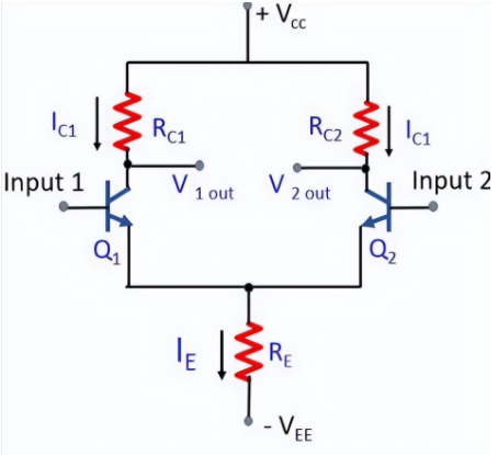
Ideally, the two transistors have similar characteristics. They share the common emitter resistor Re and the supply rails Vcc and Vee. The next step is to apply signals to the inputs and observe the outputs.
2.2 Four common input/output configurations
- Dual input, balanced output: both inputs are driven and outputs are taken from both transistors.
- Dual input, single-ended output: both inputs are driven but output is taken from a single transistor.
- Single input, balanced output: a single input is applied and outputs are obtained from both transistors.
- Single input, single-ended output: a single input is applied and the output is taken from a single transistor.
2.3 Differential operation
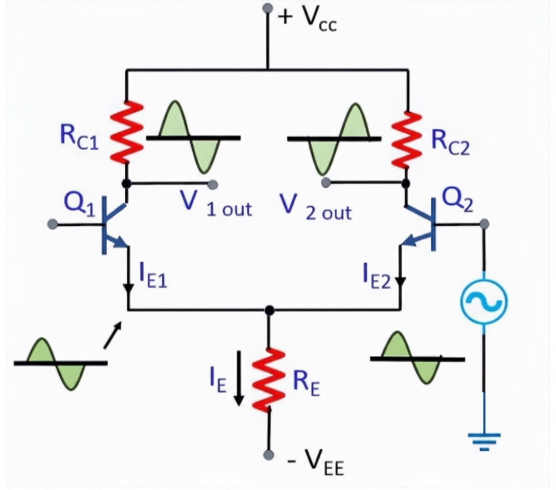
Case 1: Signal applied to Q1
Apply a signal to the base of Q1 while Q2's base is held at a constant potential. Q1 operates in two ways: as a common-emitter amplifier, producing an inverted amplified output at its collector, and as an emitter-follower, producing a noninverted signal at its emitter that is slightly smaller in amplitude.
When Q1's base receives a positive input, Q1 conducts. The voltage drop across RC1 increases, causing the collector voltage of Q1 to move negative (inverted output). The increased emitter current increases the voltage drop across RE, shifting both emitters in the positive direction. This makes Q2's base relatively more negative, reducing Q2's collector current. As RC2's voltage drop decreases, Q2's collector moves more positive, producing a noninverted output at Q2's collector corresponding to the positive input at Q1's base.
Case 2: Signal applied to Q2
When the signal is applied to Q2 with Q1's base held constant, the roles reverse: Q2 behaves as the common-emitter stage and emitter-follower, while Q1 behaves as the complementary stage. The collector of Q1 receives the inverted amplified output and the collector of Q2 receives the noninverted amplified output.
3. Differential Circuits Built with Operational Amplifiers
3.1 Differential op amp circuit
A differential amplifier amplifies the voltage difference between two input signals and is an important building block in analog integrated circuits. Differential stages often form the input of an operational amplifier. In short, a differential amplifier amplifies the difference between two input voltages.
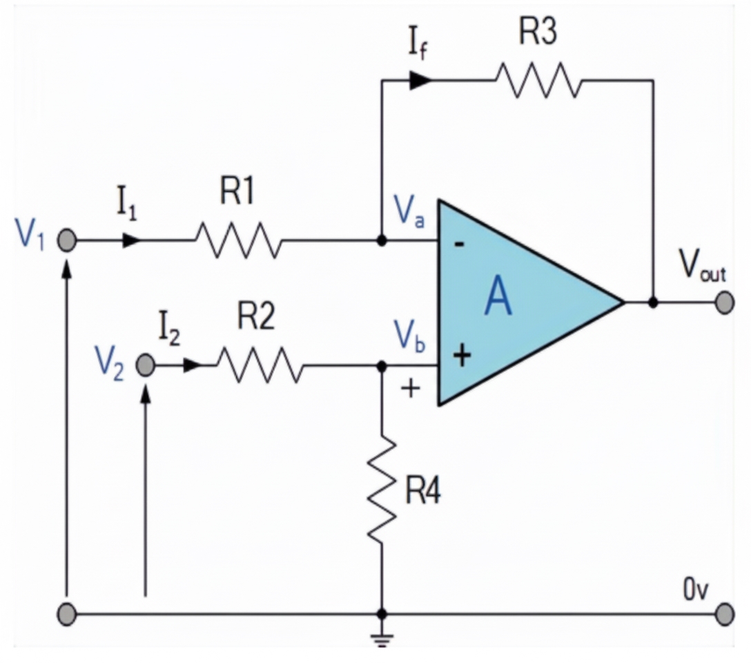
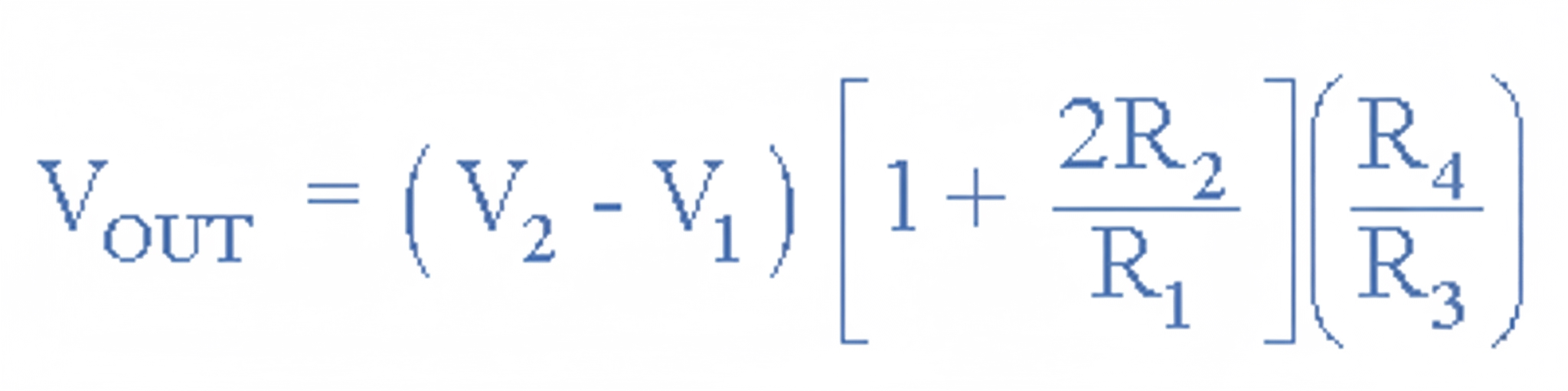
3.2 Differential amplifier transfer function
Using superposition by grounding each input in turn, the output voltage Vout can be solved. The differential amplifier transfer function is shown below.
When R1 = R2 and R3 = R4, the transfer function simplifies to:
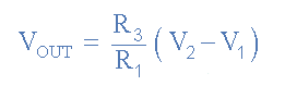
If all resistors have equal resistance R1 = R2 = R3 = R4, the circuit becomes a unity-gain differential amplifier and the voltage gain is exactly 1. The output is:
Vout = V2 - V1
Note that if V1 is higher than V2, the output will be negative; if V2 is higher than V1, the output will be positive.
3.3 Practical differential amplifier circuits
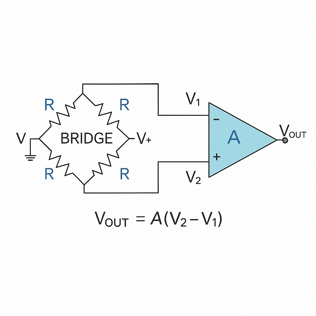
(1) Wheatstone bridge differential amplifier
A practical way to add or subtract voltages applied to the inputs is to place resistor networks in parallel with the input resistors. One common approach is to connect a Wheatstone bridge to the amplifier inputs.
(2) Light-activated differential amplifier
By comparing one input voltage to another, a standard differential amplifier can function as a differential voltage comparator. For example, one input can be tied to a fixed reference set by a resistor divider and the other input to a photoresistor (LDR). The amplifier output then becomes a function of the bridge arm that includes the LDR, producing an output that varies with light level. A simple light-activated switch using this idea will toggle a relay or drive an output when the LDR resistance crosses a set threshold.
The fixed voltage reference is provided by an R1-R2 divider and applied to the noninverting input. The threshold (trip point) is set by the feedback potentiometer VR2, and VR2 can also provide hysteresis so that the turn-on and turn-off light levels differ. The LDR forms the second input leg; its resistance changes with illumination.
The LDR can be a standard cadmium sulfide (CdS) photoresistor such as the NORP12, with a resistance around 500 ohms in bright sunlight to about 20 kohm in darkness. The LDR resistance decreases as light intensity increases, causing the voltage at the amplifier input to move above or below the switch point set by VR1. Adjusting VR1 sets the light level at which switching occurs; VR2 adjusts hysteresis. Depending on the design, the op amp output can drive a load directly or use a transistor driver to control a relay or lamp.
Replacing the photoresistor with a thermistor enables the same circuit to detect temperature instead of light. Swapping VR1 and the sensor lets the circuit detect bright/dark or hot/cold as needed.
One limitation of this differential amplifier configuration is its relatively low input impedance compared with other op amp configurations such as the noninverting amplifier. Each input source must drive current through the input resistors, so the total input impedance seen by each source is lower than an isolated op amp input. This can be acceptable for low-impedance sources like bridge networks but is undesirable for high-impedance sensors.
A remedy is to add unity-gain buffer amplifiers at each input. That yields a differential amplifier with very high input impedance and low output impedance, since the front end consists of two noninverting buffers followed by a differential stage. This arrangement forms the basis of most instrumentation amplifiers.
(3) High input impedance instrumentation amplifier
An instrumentation amplifier is a high-gain differential amplifier with high input impedance and a single-ended output. It is typically used to amplify very small differential signals from sensors such as strain gauges, thermocouples, or current-sensing devices. Unlike a standard op amp whose closed-loop gain is set by feedback from the output to an input terminal, an instrumentation amplifier uses internal resistor networks that effectively isolate its inputs from the feedback network. The common-mode rejection ratio (CMRR) of a good instrumentation amplifier can be well over 100 dB at DC.
Two noninverting amplifiers form the buffered differential input stage. Their outputs feed a differential amplifier. The differential gain of the input stage equals 1 + 2R2/R1, while common-mode gain is unity. Because the input amplifiers operate with negative feedback, the voltages at their summing nodes equal the applied input voltages. The resistor R1 between the two summing networks sees the differential input as a voltage drop; changing R1 adjusts the differential gain. The final differential amplifier stage produces an output proportional to V2 - V1 multiplied by the stage gain (which can be 1 if R3 = R4).
The overall voltage gain of the instrumentation amplifier is therefore given by the standard instrumentation amplifier formula.