Introduction
Silicon carbide (SiC) is an advanced semiconductor material with significant potential for breakthroughs in power and high-temperature electronics. This article reviews the origins, crystal structure, epitaxial growth, wafer manufacturing, device design, and packaging and modularization of SiC technology, and summarizes its key technical characteristics and application areas.
History and early development
The mineral later named moissanite was identified in a meteorite by French chemist Henri Moissan in 1891 and was recognized as silicon carbide. In the 1940s, Edward Goodrich Acheson developed the Acheson process, which produces synthetic silicon carbide by carbothermal reduction of silica and graphite at high temperatures in an electric furnace. That process marked the beginning of industrial interest in SiC as a distinct material.
Material properties and crystal structures
SiC exists in several polytypes; the most common for electronic applications are 4H-SiC and 6H-SiC. The crystal lattice is formed by alternating silicon and carbon atomic layers. Key properties that make SiC attractive for semiconductor devices include:
- Wide bandgap: Larger bandgap than silicon enables operation at higher temperatures and higher voltages, and reduces carrier recombination.
- High melting point and thermal stability: Melting point around 2700°C, enabling stable operation at elevated temperatures.
- High carrier mobility: Enables high-speed and high-frequency operation.
- High critical electric field: Allows devices to withstand higher voltages while reducing size and weight.
- Low intrinsic carrier concentration: Contributes to lower leakage currents in power devices.
- High thermal conductivity: Improves heat dissipation and thermal management in high-power applications.
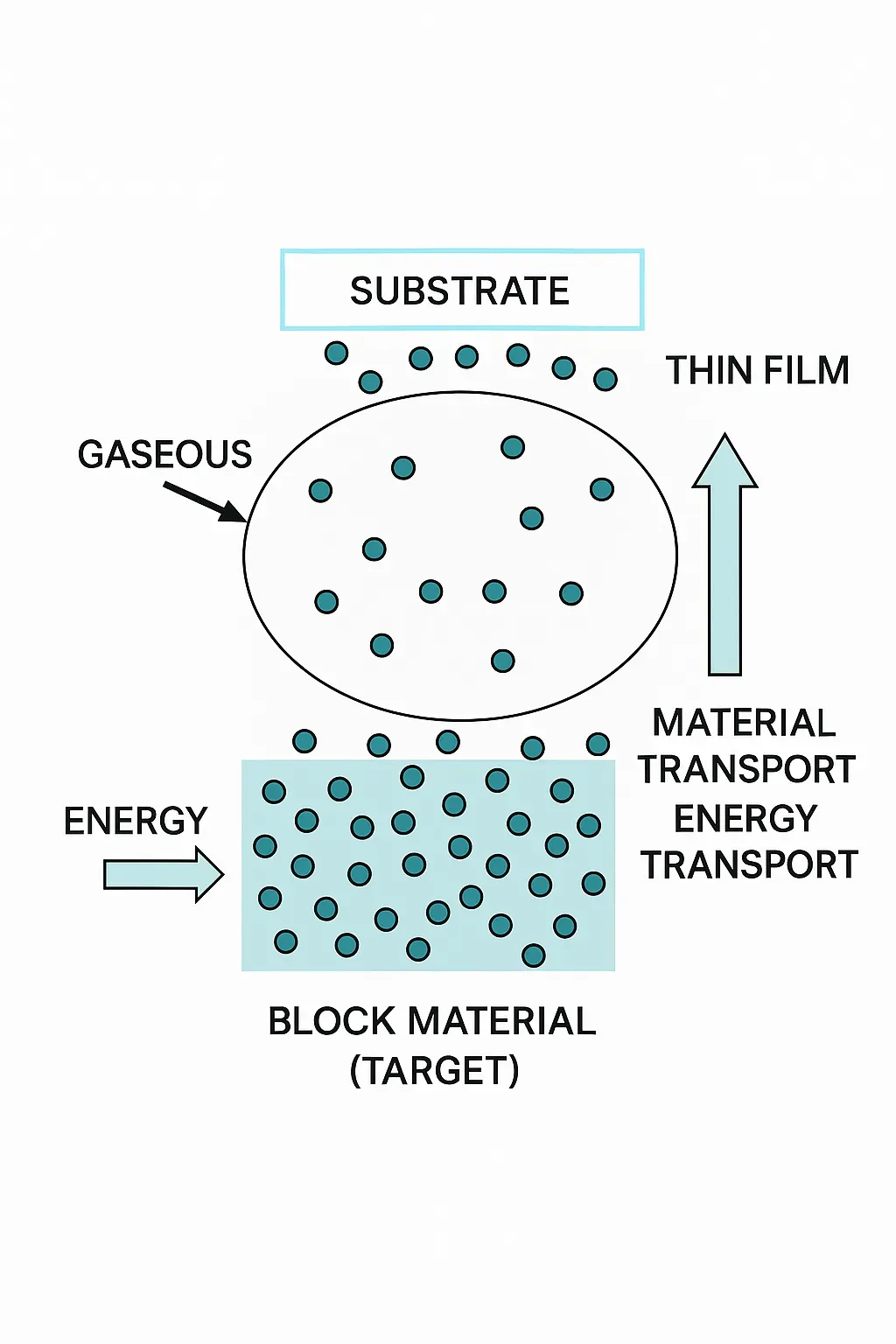
Epitaxy and thin-film growth
Epitaxial growth of SiC is a fundamental semiconductor fabrication technique used to deposit high-quality SiC layers on substrates. Typical methods include chemical vapor deposition (CVD) and physical vapor deposition (PVD). CVD-based approaches such as low-pressure CVD and gas-source epitaxy are widely used to control layer thickness, doping and crystal orientation.
Applications of SiC epitaxy include:
- Power electronics: Epitaxial SiC layers are used to fabricate power MOSFETs, Schottky diodes and other high-voltage devices, leveraging SiC's high critical field, mobility and low leakage.
- Optoelectronics: SiC's refractive index and broad spectral response support photonic devices, laser diodes and optical sensors.
- RF devices: Low loss, high mobility and high thermal conductivity make epitaxial SiC promising for RF power amplifiers, high-frequency switches and wireless communications equipment.
Substrates
SiC substrates provide the mechanical and electrical foundation for SiC device fabrication. Important substrate characteristics include:
- Wide bandgap: Supports high-temperature, high-power and high-frequency operation.
- High thermal stability and conductivity: Reduces thermal buildup and stress in high-power devices.
- High critical electric field: Enables compact high-voltage devices with improved power density.
- Good carrier mobility: Supports high-speed switching and RF operation.
Common substrate fabrication and growth methods include PVD techniques such as thermal evaporation, electron-beam evaporation and magnetron sputtering, and CVD methods where precursor gases react on the substrate surface at elevated temperature.
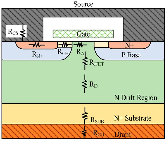
Device design considerations
SiC device design aims to exploit material advantages—wide bandgap, high thermal stability, high critical field and high carrier mobility—while addressing thermal and electric-field management. Key design focuses include:
- Structural optimization: Minimize resistance, capacitance and inductance through layout and device geometry.
- Electric-field control: Shape field distributions to maximize breakdown field and minimize on-resistance and leakage.
- Thermal management: Design heat paths and choose materials to ensure stable high-temperature operation and long lifetime.
SiC device design is critical across application areas such as power electronics (MOSFETs, Schottky diodes, power modules), optoelectronics (photodetectors, laser diodes, sensors) and RF components (power amplifiers, high-frequency switches).
Wafer manufacturing and processing
SiC wafer production is a key enabler for large-scale device manufacturing. Typical process flow includes substrate selection, epitaxial growth, post-growth processing such as chemical mechanical polishing (CMP) and oxidation, and rigorous metrology and electrical testing to ensure surface quality and crystal integrity.
Critical manufacturing technologies include:
- Epitaxy: CVD and PVD epitaxial methods to grow high-quality SiC layers.
- Wafer processing: Mechanical polishing, CMP and wafer slicing to obtain flat surfaces and precise wafer dimensions.
- Quality control: Surface inspection, X-ray diffraction and electrical characterization to ensure electrical properties and crystal quality.
Packaging and modularization
Packaging and modularization are essential steps to realize the performance and reliability advantages of SiC devices in practical systems.
Packaging functions and benefits:
- Protection: Physical protection of the device from environmental damage to improve stability and lifetime.
- Thermal management: Package design and material selection are critical to dissipate heat and maintain lower junction temperatures.
- Electrical interfaces: Provide reliable electrical connections and interfaces for signal transmission and power transfer.
- Size and integration: Packaging and module design control device footprint and volumetric density to meet integration requirements.
Key packaging and module technologies for SiC include:
- Thermal design: Heat-spreading structures and thermally conductive materials tailored for high-power, high-temperature operation.
- Material compatibility: Selection of package materials with matching thermal expansion, electrical insulation and mechanical strength.
- Lead and package structure design: Contact geometries and package architectures optimized for low inductance and reliable connections.
- Soldering and assembly processes: Robust attachment methods to ensure stable mechanical and electrical interfaces between device and package.
Applications for SiC packaging and modules span power electronics (high-power density, high-temperature power modules), optoelectronics (high-speed, high-power photonic packages), automotive electronics (high-efficiency, high-reliability automotive power systems) and high-temperature environments such as aerospace, nuclear and industrial processing.