Why is MOSFET Gate Drive Design Crucial for System Reliability?
MOSFETs (Metal-Oxide-Semiconductor Field-Effect Transistors) are fundamental components in modern power electronics, extensively employed in applications like switch-mode power supplies, motor control systems, and various power tools. Their widespread adoption is attributed to several advantageous characteristics, including rapid switching speeds, excellent high-frequency performance, high input impedance, minimal noise generation, low drive power requirements, a broad dynamic range, and a wide safe operating area (SOA).
Despite their robust performance, the gate of a MOSFET is particularly susceptible to damage if not driven correctly. Suboptimal gate-circuit design can precipitate severe consequences, leading to premature device failure or even complete system malfunctions. This guide aims to elucidate the essential functions of MOSFET gate drive circuits and present typical implementation strategies, serving as a comprehensive reference for designers.
Core Functions of an Effective Gate Drive Circuit
A well-designed MOSFET gate drive circuit serves multiple critical functions that enhance both device longevity and system stability:
● Noise Suppression: Minimizing coupled noise to boost overall system reliability.
● Turn-on Acceleration: Speeding up the MOSFET turn-on transition to reduce associated conduction losses.
● Turn-off Acceleration: Hastening the MOSFET turn-off process to minimize switching losses.
● dV/dt and di/dt Control: Limiting the rates of change of voltage (dV/dt) and current (di/dt) to protect the MOSFET and mitigate electromagnetic interference (EMI).
● Overvoltage Protection: Shielding the gate from abnormal overvoltage conditions that could lead to gate dielectric breakdown.
● Drive Capability Enhancement: Augmenting the drive signal to ensure that even small input signals can effectively control large MOSFETs.
Common Gate Drive Architectures and Their Implementation
Understanding various gate drive architectures is key to selecting the most appropriate solution for a given application, balancing performance, cost, and complexity.
Direct Drive from a Controller IC
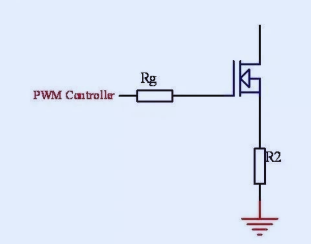
One of the simplest and most common gate drive methods involves directly connecting the MOSFET gate to the output of a power supply or a Pulse Width Modulation (PWM) controller IC. In this approach, where minimal additional circuitry is used, careful high frequency pcb layout is paramount. It is crucial to:
● Shorten the Trace: Minimize the length of the conductive path between the IC and the MOSFET gate.
● Increase Trace Width: Widen the trace to reduce its inherent resistance and inductance.
● Proximity Placement: Position the gate resistor as close as possible to the MOSFET gate terminal.
These measures are essential for minimizing parasitic inductance, which can cause unwanted oscillations, and for effectively suppressing noise in the gate loop.
A critical consideration for direct drive is the inherent drive capability of the PWM controller. For larger MOSFETs, which possess significant gate capacitance, a controller with insufficient output current may struggle to charge and discharge the gate quickly enough. This can result in slower switching transitions, leading to increased switching losses and potentially improper MOSFET operation.
Enhancing Drive Capability with External Transistor Stages
When the internal drive current provided by a controller IC is insufficient for the demands of the MOSFET—particularly for high-power applications or larger devices—external transistor stages can be integrated to boost the drive current.
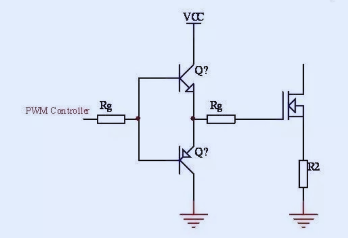
This augmentation significantly increases the current available during the turn-on phase, allowing for a faster charging of the gate capacitance. Similarly, it can dramatically accelerate the turn-off process by providing a low-impedance path for the gate capacitance to discharge. This enhanced control over switching transients directly contributes to reduced power loss and improved overall efficiency. In terms of physical layout, these external driver transistors should be placed in close proximity to the MOSFET gate to minimize parasitic inductance and enhance the circuit's immunity to noise.
Accelerating MOSFET Turn-off Speed
To achieve a more rapid turn-off specifically, a lower-impedance discharge path for the MOSFET's gate capacitance is often required. A widely adopted technique involves adding a speed-up diode in parallel with the gate resistor.
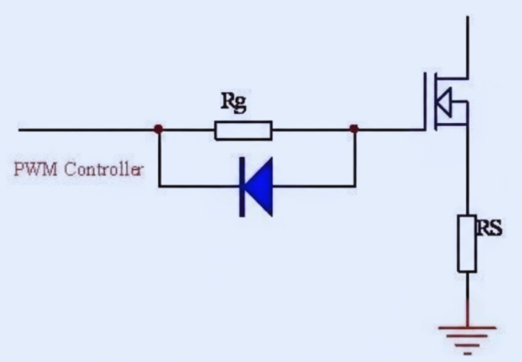
When the gate drive signal transitions low, the diode becomes forward-biased and conducts current once the voltage drop across the gate resistor exceeds the diode's forward voltage. This effectively bypasses the gate resistor, providing a significantly larger discharge current for the gate capacitance. As the gate voltage continues to fall, the diode's influence gradually diminishes. This configuration substantially reduces the MOSFET's turn-off delay time. A limitation of this approach is that the gate discharge current still flows through the output impedance of the driving IC.
PNP Accelerated Turn-off Driver
The PNP accelerated turn-off circuit is a widely implemented technique designed to provide a more direct and efficient discharge path for the gate capacitance. In this configuration, the PNP transistor momentarily creates a low-resistance path between the gate and source terminals during the turn-off transition, enabling a very fast discharge of the gate capacitance. A diode is typically included in the circuit, serving to protect the transistor's base-emitter junction and to establish a return path and bias for the conduction current.
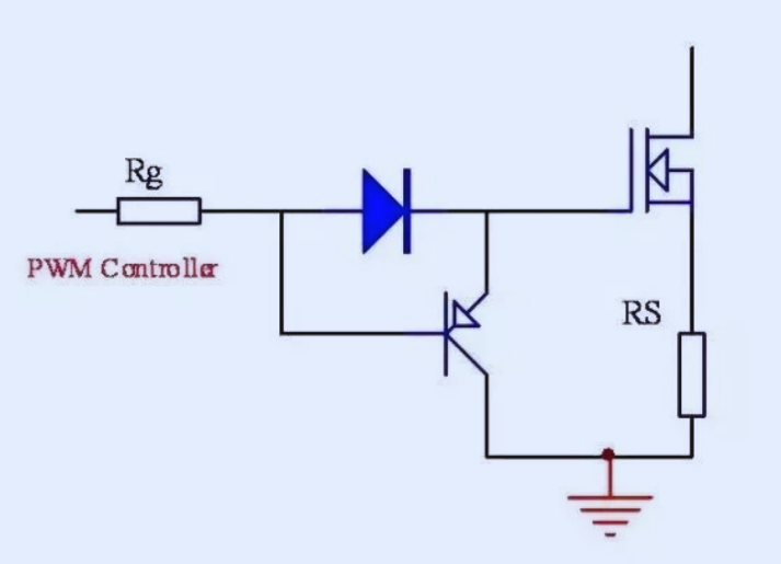
This circuit effectively mimics a push-pull operation, delivering a clear and pronounced acceleration benefit during turn-off. A notable limitation of this design is that the gate signal is driven through two PN junctions (the base-emitter of the PNP and the diode), meaning the gate voltage cannot be driven precisely to 0 V referenced to the source during the off state.
Advanced Gate Drive Techniques for Complex Scenarios
Beyond basic drive circuits, specific applications demand more sophisticated solutions, such as driving MOSFETs when their source terminal is not referenced to ground, or when galvanic isolation is a requirement.
Driving MOSFETs with a High-Voltage Source Reference
When a MOSFET operates in a configuration where its source terminal is at a high potential relative to the system ground (e.g., in a high-side switching application), the gate drive circuit must be biased to "float" with the source voltage. This means that the gate drive voltage must swing relative to the MOSFET's source potential, not a fixed ground reference. Achieving this requires either a dedicated floating drive supply or a bootstrap arrangement that dynamically references its output to the MOSFET source.
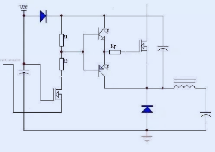
The critical aspect here is ensuring the drive supply's reference point moves in tandem with the MOSFET's source. This ensures that the voltage difference between the gate and source (Vgs) remains correctly maintained for proper switching, regardless of the common-mode voltage at the source.
Isolated Gate Drive Utilizing a Transformer
For applications demanding complete galvanic isolation between the control circuitry and the MOSFET gate, or for driving high-side MOSFETs in high-voltage environments, transformer-based gate drivers are an excellent solution. Transformer isolation physically separates the controller from the MOSFET gate, making it suitable for both low- and high-voltage circuits where safety or noise immunity is paramount.
In such circuits, a coupling capacitor is typically included. Its purpose is to provide a DC reset path for the magnetizing flux within the transformer core. Without this capacitor, the core could accumulate flux, leading to saturation and improper operation over time. Additionally, a resistor in series with this capacitor is often employed to dampen any LC (inductor-capacitor) ringing that might occur due to abrupt changes in the duty cycle, thereby ensuring cleaner drive signals.
Conclusion
MOSFETs are indispensable components in modern power electronics, but their reliable operation hinges on meticulously designed gate drive circuits. As highlighted in this overview, the gate is a sensitive part of the device, and inadequate gate drive can lead to significant performance issues and system failures. By understanding the common functions of gate drive circuits—such as noise suppression, accelerating switching transitions, and overvoltage protection—designers can implement robust solutions.
Whether employing a straightforward direct drive from a controller IC, augmenting drive current with external transistors, utilizing speed-up diodes, or deploying advanced techniques like PNP accelerated turn-off drivers, floating supplies, or transformer isolation, the choice depends heavily on the specific application requirements. Adhering to proper PCB layout practices and carefully selecting components are paramount to ensuring fast, efficient, and reliable MOSFET switching, ultimately contributing to the overall stability and longevity of the power system.