Residual stress is a major concern in MEMS development. Residual stress in MEMS devices significantly affects device performance and reliability. Based on their origins, residual stresses are generally classified into intrinsic stress and thermal mismatch stress. Intrinsic stress arises from lattice mismatch and other deposition-related factors, while thermal mismatch stress results from differences in coefficients of thermal expansion between materials.
What is intrinsic stress?
Intrinsic stress, also called internal stress, refers to stress that exists inside a material at room temperature with no external load. It can be either compressive or tensile. Intrinsic stress is particularly significant in thin films used in MEMS. When intrinsic stress is nonuniform through the film thickness, a stress gradient is produced. If the stress gradient is not counteracted by the film's elastic modulus, the film will deform, which can induce wafer warpage or cause film delamination and cracking. Besides single-layer films, composite film stacks require careful attention to combined stresses. Many MEMS structures, such as suspended membranes and cantilevers, are composite films. The key in such composite-film designs is stress matching and compensation between layers.
Intrinsic stress mainly originates during film deposition. Deposition method, temperature, pressure, and rate can all produce lattice mismatch and thus intrinsic stress. For example, gold (Au) films deposited by evaporation typically have lower intrinsic stress than those deposited by magnetron sputtering. Among materials commonly used in MEMS, almost none have zero intrinsic stress. Therefore, process development focuses on producing low-stress films. Low-pressure chemical vapor deposition (LPCVD) is commonly used to deposit silicon nitride films. Controlling temperature, pressure, reactant gas ratios, and reaction time is necessary to achieve low-stress SiNx; this typically requires silicon-rich conditions, i.e., a high DCS/NH3 ratio. Note that temperature differences between the LPCVD tube inlet/outlet and the tube center can cause significant stress variation for SiNx deposited in the same furnace; increasing the center temperature can help reduce wafer-to-wafer stress differences.
What is thermal mismatch stress?
Thermal mismatch stress, also called thermal stress, refers to interfacial stress caused by differences in coefficients of thermal expansion (CTE) between different materials. Two conditions must be met to generate thermal mismatch stress: first, two materials with different CTEs must be present; second, a temperature change must occur. Thermal mismatch stress is unavoidable during MEMS fabrication and operation. If temperature changes during fabrication or use induce nonelastic (plastic) deformation in the device or films, this can cause fabrication failures or reliability issues. Therefore, the thermal budget is progressively reduced as the process proceeds; high-temperature steps are generally confined to the earliest process steps.
Unlike intrinsic stress, thermal mismatch stress can sometimes be exploited. Thermal actuators in MEMS use the CTE difference between film layers to drive cantilevers. In a bilayer thermal actuator, temperature rise causes the cantilever to bend toward the layer with the lower CTE; when temperature returns to baseline, the cantilever returns to its original position.
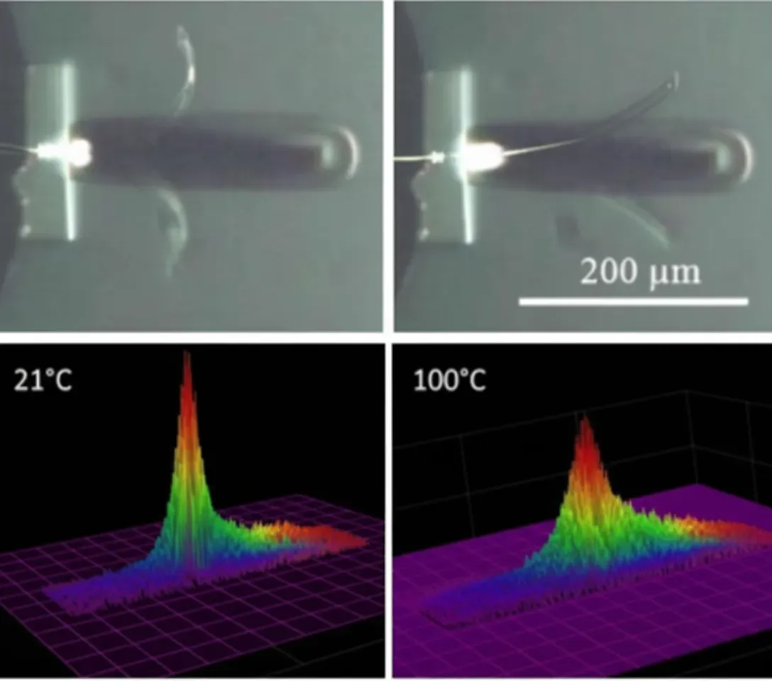
Figure 1 Thermal actuator
How to achieve stress matching?
Stress matching is one of the most important considerations in MEMS process design. Without reasonable film stress matching, MEMS devices will almost always fail. The following example illustrates stress matching methods for a metal cantilever. The selected materials are chromium (Cr) and gold (Au). Cr films deposited by magnetron sputtering have an intrinsic stress of 1000 MPa and a CTE of 4.9e-6/°C. Au films deposited by magnetron sputtering have an intrinsic stress of 200 MPa and a CTE of 14.1e-6/°C.
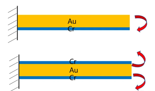
Figure 2 Schematic of stress-matching model
3.1 Two-layer composite film
With Cr as the bottom layer and Au as the top layer, intrinsic stress creates a stress gradient that bends the composite toward the higher-stress direction, i.e., downward. Considering thermal stress, Cr has a smaller CTE than Au, so the composite also bends toward the lower-CTE direction, again downward. In practice, Cr is often used as an adhesion layer for Au. Analysis shows that both intrinsic and thermal stresses cause the composite to deform, which is detrimental to device fabrication. Typical solutions are to minimize Cr film intrinsic stress and thickness and to increase Au thickness to resist deformation.
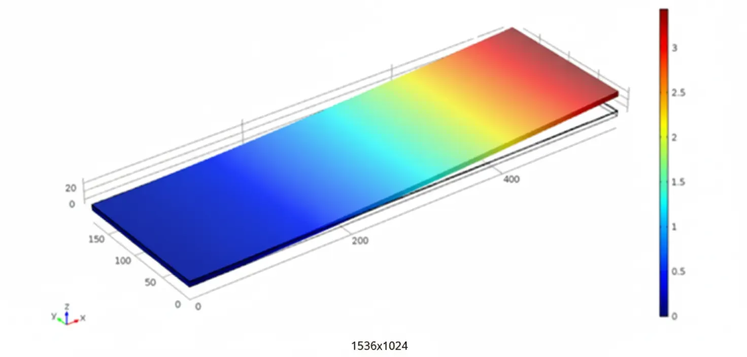
Figure 3 Mechanical simulation of stress matching
3.2 Three-layer composite film
With Cr as the bottom layer, Au in the middle, and Cr on top, a sandwich structure is formed. Considering intrinsic stress gradients, the middle Cr layer will bend toward both Au layers, allowing intrinsic stress cancellation. Considering thermal stress, Cr's smaller CTE causes the middle Cr layer to bend toward both Au layers, enabling thermal stress compensation as well. The only practical consideration is that the top and bottom layers should be as similar in thickness as possible to achieve simultaneous compensation of intrinsic and thermal stresses.
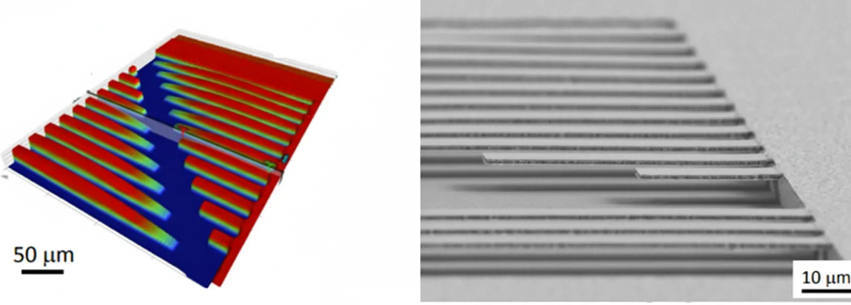
Figure 4 Au-TiW bilayer stress-matching simulation and SEM (reference: 10.1016/j.matdes.2016.06.003)
In practical process design and fabrication, the analysis above indicates that odd-numbered layer combinations are generally superior to even-numbered combinations for stress compensation. In MEMS film design, especially when both tensile and compressive stresses coexist, the priority is to reduce the intrinsic stress of individual layers. Once individual layers have low stress, stress compensation and matching across layers are the key to successful device design and fabrication.