Overview
A sensor manufactured using MEMS technology is referred to as a MEMS sensor. A typical sensor consists of four main parts: a sensitive element, a transduction element, conversion circuitry, and an auxiliary power supply. In MEMS acoustic sensors, the MEMS chip serves as the sensing element that detects signals, while an ASIC chip performs signal processing and conversion. The MEMS chip and the ASIC are the most technologically and economically significant components of a MEMS sensor.
MEMS Chip vs Integrated Circuit Chip
Both MEMS chips and integrated circuit (IC) chips commonly use silicon as the wafer substrate and share many fabrication steps such as lithography, thin film deposition, etching, and doping. However, MEMS chips integrate mechanical structures that control physical phenomena and convert them into electrical signals, enabling mechanical-electrical interaction. Traditional IC chips implement circuits by placing transistors, resistors, capacitors, and interconnects into a semiconductor substrate, and they generally pursue more advanced process nodes to increase component density and performance.
MEMS devices typically contain mechanical structures with feature sizes from 1 to 100 micrometers, and common device dimensions range from about 20 micrometers to 1 millimeter. MEMS fabrication emphasizes process development for mechanical structures rather than pushing the most advanced lithography node. Because MEMS device requirements vary widely, there is no single unified process that covers all MEMS devices; this "one product, one process" characteristic limits mass-production scalability. Developing more generic MEMS process flows is therefore a key focus in MEMS research and manufacturing.
What Is an ASIC and How MEMS ASICs Differ
MEMS chips convert the measured physical quantity into electrical changes such as resistance or capacitance. The ASIC converts these small analog changes into usable electrical signals, performing functions such as conversion, amplification, filtering, and conditioning. Because the analog output from MEMS devices is often extremely weak or produced under unconventional conditions, general-purpose ASICs may not meet MEMS requirements. This has led to a shortage of MEMS-specific ASICs in the industry. Designing ASICs tailored for MEMS sensors is therefore a critical shared technology for MEMS development.
Major MEMS Manufacturing Processes
MEMS processing is based on conventional semiconductor process steps such as film deposition, photolithography, etching, and bonding. Key process technologies used in MEMS fabrication include SOI wafers, wafer bonding, bulk micromachining, surface micromachining, LIGA, wet etching, deep reactive ion etching (DRIE), and atomic layer deposition (ALD).
SOI Wafers
SOI stands for Silicon On Insulator. SOI wafers include a buried oxide layer between the top silicon and the backing substrate. In MEMS, the oxide layer can act as an etch stop, enabling the formation of complex three-dimensional structures.
Wafer Bonding and Thermal Release Carrier Processes
Wafer bonding and thermal release carrier methods enable handling and processing of thinned wafers by using support wafers or temporary bonding films. Wafer bonding is a wafer-level packaging technique used for MEMS, NEMS, microelectronics, and optoelectronics to ensure mechanical stability and hermetic sealing.
Wafer bonding joins two substrates, such as silicon-to-silicon or silicon-to-glass, under conditions of temperature, pressure, or voltage so that molecular forces or chemical bonds form at the interface. Wafer bonding is broadly categorized as either direct bonding or bonding through an intermediate layer. Direct bonding does not use adhesives and relies on intermolecular forces activated by heat treatment, while intermediate-layer bonding uses adhesives or other bonding layers.
Three MEMS Fabrication Approaches
The main MEMS fabrication approaches are bulk micromachining, surface micromachining, and LIGA. Bulk and surface micromachining are the most widely used and mature.
Bulk Micromachining
Bulk micromachining creates mechanical structures by anisotropic or isotropic etching of the silicon substrate. It is characterized by simple equipment and lower investment, but is typically limited to simpler shapes and devices with smaller aspect ratios. Bulk micromachining is a subtractive process that consumes silicon and generally targets silicon substrates for processing. It includes both wet and dry etching and is a key method for producing three-dimensional MEMS structures.
Surface Micromachining
Surface micromachining relies on thin film deposition, photolithography, and etching. It commonly uses a sacrificial layer that is later removed to release mechanical structures. Typical steps include depositing structural and sacrificial films, patterning by photolithography, and removal of the sacrificial layer to free the structure. Surface micromachining is capable of fabricating microstructures within approximately 10 micrometers thickness and multi-layer suspended structures, but it requires careful control of mechanical properties and solutions for stiction, residual stress, friction, and actuation.
LIGA
LIGA stands for Lithographie, Galvanoformung, Abformung and enables the fabrication of high aspect ratio parts from metals or plastics, which can be difficult for bulk or surface micromachining. LIGA requires high-energy radiation such as X-rays produced by synchrotron sources for deep X-ray lithography, so the equipment and investment are significant. The LIGA process includes mask fabrication, deep X-ray lithography, micro-electroforming, and micro-replication.
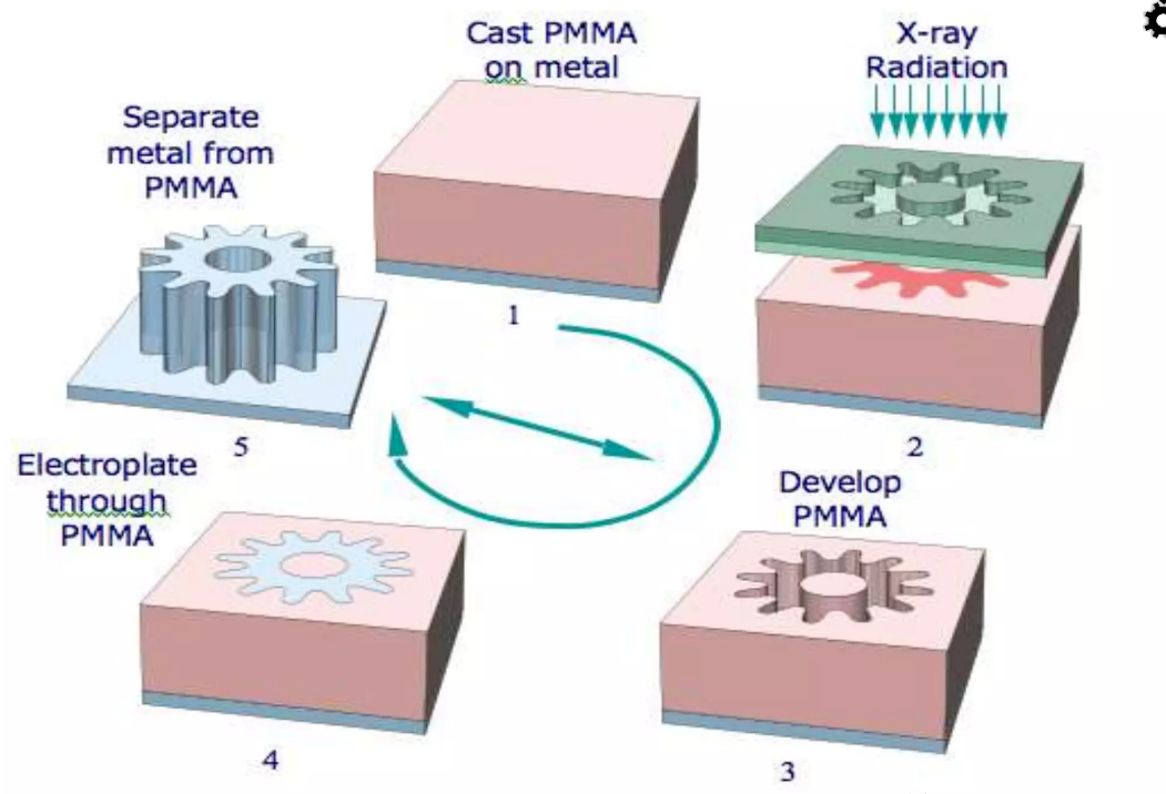
Figure: LIGA process flow
Wet Etching and Deep Reactive Ion Etching (DRIE)
Silicon wet anisotropic etching is one of the earliest micromachining techniques. Wet etching uses a chemical solution to react with the material and remove exposed areas, and remains widely used in devices such as accelerometers and pressure sensors due to its relative simplicity and lower cost. Common anisotropic wet etchants include potassium hydroxide (KOH), tetramethylammonium hydroxide (TMAH), and hydrazine-based solutions.
Dry deep etching, typically implemented with deep reactive ion etching (DRIE), provides high aspect ratio anisotropic etching and is increasingly used in bulk micromachining. DRIE can etch polysilicon, silicon dioxide, metals, and other materials by selecting appropriate etch gases and passivation atmospheres, making it highly valuable for many MEMS applications.
DRIE features include higher etch rates than typical wet etching (often 2 to 15 times faster), high aspect ratios capable of etching through full wafer thickness, etch profiles largely independent of crystal orientation, and high selectivity between the etched material and mask or stop layers. DRIE often uses fluorinated gases such as SF6 to generate a reactive plasma and a passivation gas to convert isotropic etching to anisotropic etching, enabling deep vertical profiles.
Deep Silicon Etching
The Bosch process, which alternates between etching and passivation steps, combines the advantages of anisotropic and isotropic etching and has become a mainstream method for deep silicon etching. By repeating cycles of silicon etch and polymer deposition followed by removal of the bottom polymer layer, deep vertical etches can be achieved. The scalloped sidewall pattern produced by the cyclic process is commonly called a "scallop morphology."
Thin Film Deposition
Atomic layer deposition (ALD) deposits material one atomic layer at a time by cycling precursor exposure and purge steps, relying on surface reactions with the substrate. ALD enables precise nanoscale film thickness control and conformal coverage in high-aspect-ratio features such as deep holes and sidewalls. It is useful for forming uniform films in deep etch processes and for depositing controlled films on recesses or pores.
Conclusion
MEMS sensors are present across consumer electronics, automotive systems, industrial automation, and medical devices. Industry data indicate that products manufactured using MEMS technology account for a large share of semiconductor sensor revenue, and MEMS devices represent a substantial portion of global sensor shipments, underscoring the broad application scope of MEMS technology.
MEMS manufacturing equipment and processes are largely at the micrometer scale and do not generally require the most advanced semiconductor nodes. Currently, advanced economies have not restricted access to MEMS manufacturing equipment in the Chinese market. MEMS technology therefore represents an important segment for growth and development within the Chinese semiconductor ecosystem.