What is Selective Soldering and Why is it Essential?
Selective soldering represents a specialized technique utilized in the assembly of printed circuit boards (PCBs) to precisely solder specific through-hole components. In contrast to wave soldering, which processes all components in a single pass, selective soldering focuses exclusively on designated areas. This makes it an optimal choice for mixed-technology boards that incorporate both surface-mount (SMT) and through-hole (THT) components. This method’s inherent precision significantly reduces thermal stress on sensitive parts and minimizes the potential for defects.
The significance of selective soldering stems from its capability to accommodate contemporary PCB designs, which frequently integrate a diverse array of component types. With the ongoing miniaturization of electronic devices, manufacturers require a process that can solder localized regions without adversely affecting adjacent components. By mastering selective soldering, manufacturers can achieve superior quality, mitigate PCB board cost, and enhance the overall reliability of their PCB assemblies.
Deconstructing the Selective Soldering Process
The selective soldering process encompasses several critical stages to ensure accurate and dependable solder joints.
Step-by-Step Operation
● Preheating: Initially, the PCB undergoes preheating to a specific temperature, typically ranging from 80°C to 120°C. This step is crucial for minimizing thermal shock when the molten solder is applied. Preheating also activates the flux, which plays a vital role in cleaning the surfaces to facilitate better solder adhesion.
● Flux Application: Flux is then precisely applied to the targeted areas. Its purpose is to remove oxides and ensure proper wetting of the solder. This stage is paramount for creating robust joints and preventing common defects such as inadequate wetting.
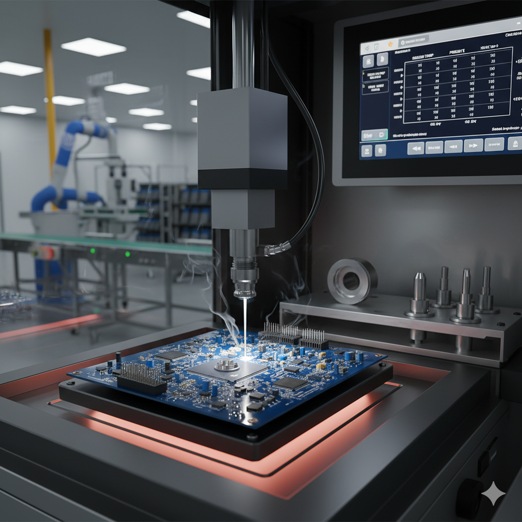
● Soldering: A highly accurate solder nozzle or fountain then moves to the designated through-hole pins, dispensing molten solder (often maintained at temperatures between 260°C and 300°C) to form the electrical connections. The movement of the nozzle is precisely controlled by specialized software to ensure consistent accuracy.
● Cooling: Following the soldering operation, the PCB is allowed to cool gradually. This controlled cooling process allows the solder joints to solidify properly and helps prevent thermal stress or the formation of cracks.
This entire process is predominantly automated, frequently employing programmable machinery to ensure uniformity across extensive production runs. By meticulously controlling parameters such as solder temperature, nozzle velocity, and preheat levels, manufacturers can achieve optimal results for a wide variety of board design
Selecting the Appropriate Selective Soldering Equipment
Choosing the correct selective soldering equipment is paramount for consistently achieving high-quality results.
Essential Equipment Considerations
● Nozzle Varieties: A range of nozzle types is available, each suited for different applications; for instance, mini-wave nozzles are ideal for small pins, while larger nozzles accommodate bigger components. It is important to ensure that the chosen equipment supports interchangeable nozzles to provide operational flexibility.
● Automation Degree: Fully automated systems, with their programmable controls, offer exceptional precision and repeatability, making them ideal for high-volume manufacturing. For smaller production runs or prototyping, semi-automated systems may be sufficient.
● Temperature Control: Seek equipment that provides highly precise temperature regulation (typically within ±1°C) to maintain consistent solder quality and prevent unintended overheating of components.
● Compatibility: Verify that the machine can accommodate your specific PCB sizes and thicknesses, as well as the particular solder alloys you intend to use, including various lead-free options.
● Maintenance and Support: Prioritize equipment from manufacturers who offer readily available spare parts and dependable technical support to minimize potential downtime during critical production periods.
Investing in top-tier selective soldering equipment can significantly reduce the occurrence of defects and enhance overall production efficiency. For example, advanced systems are capable of processing up to 500 solder joints per hour, depending on the complexity of the board, rendering them an invaluable asset for large-scale manufacturing operations.
Optimizing PCB Design for Selective Soldering
Designing a PCB with the selective soldering process in mind can proactively mitigate numerous PCB assembly challenges.
Key Design Recommendations
● Component Separation: Ensure ample clearance between through-hole components and adjacent surface-mount parts to prevent unwanted thermal interference. A minimum spacing of 2-3 mm is frequently advised.
● Pad and Hole Sizing: Verify that through-hole pads and their corresponding holes are correctly dimensioned for the specific components. For instance, a hole diameter approximately 1.2 times the lead diameter typically facilitates proper solder flow.
● Thermal Relief Implementation: Incorporate thermal relief patterns on pads that are connected to extensive ground planes. This measure helps prevent excessive heat dissipation during soldering, promoting uniform heating and the formation of robust joints.
● Component Alignment: Arrange components such that the solder nozzle can access all targeted areas without any physical obstructions. Avoid positioning tall components in the direct path of the nozzle's movement.
● Flux Compatibility: Design the board to be compatible with the specific type of flux employed in selective soldering, ensuring that any residual flux will not negatively impact other components or subsequent testing procedures.
By integrating these design considerations early in the development cycle, you can significantly reduce the potential for defects and ensure a smoother selective soldering operation. It is always advisable to simulate the proposed soldering path during the design phase to identify and address any potential challenges before full-scale production commences.
For more information of selective soldering, see our PCB Soldering guide: The Definitive Guide to PCB Soldering: Standards, Techniques, and Strategic Implementation
Identifying and Understanding Common Selective Soldering Defects
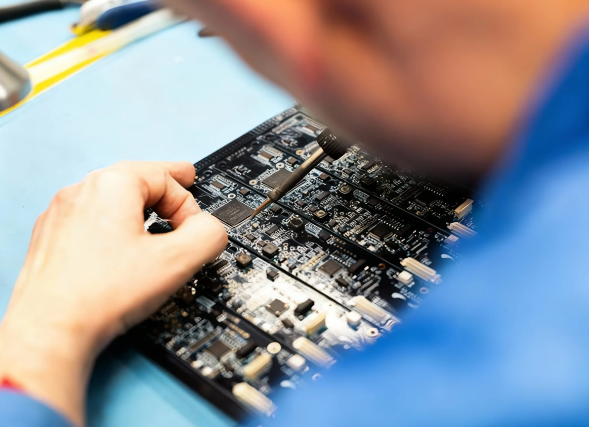
Even when employing the finest equipment and adhering to optimal design practices, selective soldering defects can still emerge. Early recognition of these issues is crucial for maintaining product quality.
Frequent Soldering Imperfections
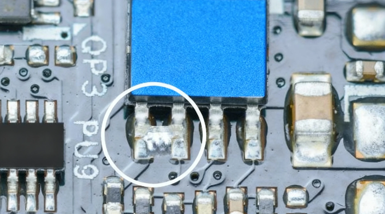
● Insufficient Solder: This defect occurs when an inadequate amount of solder is applied, leading to weak or compromised joints. It is often a result of low solder temperature (below 260°C) or insufficient flux activation.
● Solder Bridging: Excess solder can inadvertently create unintended electrical connections between adjacent pins. This typically stems from improper nozzle alignment or an excessive solder flow rate.
● Poor Wetting: If the solder fails to adhere properly to the pad or component lead, it can result in unreliable joints. This issue is commonly attributed to contamination on the surfaces or insufficient activation of the flux.
● Thermal Damage: Prolonged or excessive heating (above 300°C) can inflict damage upon components or the PCB substrate itself, potentially leading to delamination or localized burning.
● Solder Balls: Small, spherical formations of solder can appear around the joint. These are often caused by rapid cooling or improper flux application, posing a potential risk of short circuits.
Routine inspection, utilizing either visual checks or automated optical inspection (AOI) systems, can effectively aid in detecting these defects. For example, a joint with insufficient solder might appear dull or incompletely formed under magnification, whereas bridging can be readily identified as an unintended connection between adjacent pins.
Troubleshooting Tips for Flawless Selective Soldering Results
When defects do occur, effective troubleshooting in selective soldering can conserve considerable time and resources.
Practical Solutions for Common Issues
● Insufficient Solder: Verify and, if necessary, increase the solder temperature to within the recommended range (260°C-300°C). Also, confirm that the preheat temperature is adequate (around 100°C) to properly prepare the board. Ensure the nozzle is clean and consistently dispensing the correct volume of solder.
● Solder Bridging: Adjust the nozzle's position and consider reducing the solder flow rate. Review the PCB design to confirm sufficient spacing between pins (at least 2 mm). A slower nozzle movement speed can also help prevent excessive solder accumulation.
● Poor Wetting: Confirm that the flux is fresh and applied uniformly across the target area. Thoroughly clean the PCB surface to remove any contaminants, such as dust or grease. If the problem persists, an extended preheat time might be necessary to fully activate the flux.
● Thermal Damage: Closely monitor both the soldering temperature and the duration of solder application. Utilize a machine with precise controls to avoid exceeding 300°C for more than a few seconds. Incorporate thermal relief designs into your PCB layout to better manage heat distribution.
● Solder Balls: Optimize the cooling rate to prevent the rapid solidification of excess solder droplets. Ensure that the amount of flux applied is appropriate—too much can lead to spattering. Regularly clean the soldering area to remove any stray solder particles.
Maintaining detailed documentation of each troubleshooting step and its outcome can be invaluable for identifying recurring patterns and preventing future issues. Additionally, performing routine maintenance on your selective soldering equipment—such as cleaning nozzles and calibrating temperature sensors—can significantly reduce the likelihood of manufacturing defects.
The Advantages of Expertise in Selective Soldering for PCB Assembly
Achieving mastery in the selective soldering process confers numerous benefits for PCB assembly, particularly within the dynamic landscape of today's electronics industry.
Key Benefits for Manufacturers
● Enhanced Precision: Selective soldering targets specific areas, thereby mitigating the risk of damage to nearby components and ensuring the formation of high-quality solder joints.
● Cost Efficiency: By minimizing defects and reducing the need for rework, this process effectively lowers overall production costs. It also diminishes the reliance on manual soldering, resulting in labor cost savings.
● Versatility: This technique is well-suited for a broad spectrum of PCB designs, including those featuring mixed technologies or high-density component layouts.
● Improved Reliability: Properly executed solder joints enhance the durability and operational performance of the final electronic product, leading to a reduction in field failures.
For manufacturers engaged in high-mix, low-volume production, selective soldering provides the flexibility required to adapt to diverse designs without compromising on quality. This inherent adaptability can serve as a significant competitive advantage in delivering dependable electronic products to the market.
Conclusion: Elevate PCB Assembly Through Selective Soldering
Selective soldering is a transformative technique in PCB assembly, offering unparalleled precision, efficiency, and reliability for intricate board designs. By thoroughly understanding the selective soldering process, making informed investments in the right equipment, optimizing PCB layouts, and developing expertise in troubleshooting, you can significantly enhance your manufacturing outcomes. Whether you are addressing common defects or fine-tuning your operational setup, the comprehensive tips and best practices outlined in this guide provide a robust foundation for achieving success.
Begin implementing these strategies today to elevate the quality of your PCB assemblies. With selective soldering, you are not merely assembling circuit boards; you are meticulously crafting the future of electronics with exceptional accuracy and dedicated attention.


