Introduction
Stencil printing serves as the foundational process in surface mount technology assembly, particularly for high-density PCBs where component pitches continue to shrink. Achieving precise solder paste deposition ensures reliable joints for fine-pitch devices like BGAs, QFNs, and 0201 passives. Poor printing leads to defects such as bridging, insufficient solder, or tombstoning during reflow, compromising yield and reliability. Advanced techniques in stencil printing for high density PCBs address these challenges by optimizing aperture geometry and process parameters. This article explores practical strategies to enhance print quality, focusing on troubleshooting common issues faced by assembly engineers. By mastering these methods, teams can achieve consistent results in demanding applications.
Why Stencil Printing Matters for High-Density SMT Assembly
High-density SMT demands exceptional precision because component lead spacings often fall below 0.4 mm, amplifying the impact of paste volume variations. Inconsistent deposits disrupt solder paste reflow optimization, leading to voids, head-in-pillow defects, or open joints post-reflow. Engineers must prioritize stencil printing as it directly influences downstream processes like placement and thermal profiling. Industry standards like IPC-7525C outline guidelines for stencil fabrication that support these tight tolerances. Troubleshooting starts here, as print defects account for a significant portion of assembly failures in production runs. Effective stencil strategies not only boost first-pass yields but also reduce rework costs in high-volume manufacturing.
Technical Principles of Advanced Stencil Printing
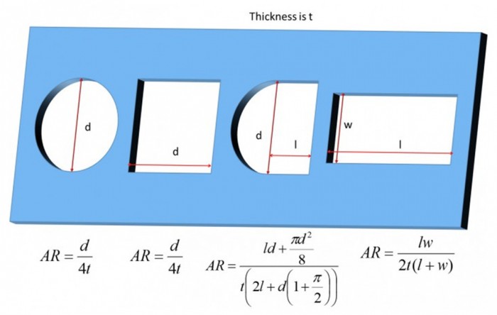
Stencil printing relies on controlled transfer of viscous solder paste through laser-cut or electroformed apertures onto PCB pads. Key principles include paste release efficiency, governed by the area ratio of aperture opening to wall surface area, as detailed in IPC-7525C. For high-density designs, maintaining an optimal area ratio prevents paste retention in small apertures, ensuring clean snap-off. Squeegee mechanics, including blade pressure and speed, shear the paste uniformly across the stencil, minimizing skips or smearing. Paste rheology, with its thixotropic properties, allows flow under shear but holds shape after deposition. Understanding these interactions helps engineers predict and mitigate issues like slumping in humid environments.
Advanced aperture designs revolutionize paste control for fine-pitch components. Traditional rectangular apertures struggle with volume consistency on small pads, prompting shapes like trapezoidal or scooped profiles to reduce trapped paste. U-shaped apertures prove effective for QFN thermal pads, channeling paste outward to avoid excess center buildup during reflow. Overlapping or home-plate configurations for BGA arrays promote uniform release across dense arrays. Electro-polishing aperture walls smooths surfaces, enhancing release while nano-coatings further minimize adhesion. These designs, aligned with stencil printing for high density PCBs, demand precise fabrication to avoid burrs that trap particles.
Optimizing Printing Parameters for Reliable Deposits
Process parameters form the backbone of repeatable stencil printing. Squeegee angle, typically set near 45 degrees, balances shear force and gasketing against the PCB. Print speed influences paste rollout, where slower rates aid fine features but risk drying, while faster passes suit larger apertures. Snap-off distance and dwell time control separation, preventing stringing or bridging between pads. Printer alignment verification using fiducials ensures sub-25 micron overlay accuracy critical for high-density boards. Regular stencil cleaning with lint-free materials maintains aperture integrity, as residue buildup exacerbates defects.
Solder paste selection ties directly to printing success. Type 4 or finer metal powders suit high-density applications, offering better stencil life and reduced agglomeration. Viscosity must match printer capabilities, with slump tests confirming stability under production conditions. Environmental controls, like temperature and humidity between 20-25C and 40-60% RH, stabilize paste performance. Pre-conditioning paste via kneading ensures homogeneity before loading. These steps in solder paste reflow optimization start at printing, setting the stage for uniform melting and wetting.
Best Practices and Troubleshooting in High-Density Printing
Implement step stencils for mixed-pitch boards, featuring thicker foils over large pads and thinner sections for fine-pitch areas to equalize volume. High-tension frames reduce flexing during printing, vital for warpage-prone substrates. SPI (solder paste inspection) post-print quantifies volume, height, and position, flagging outliers early. Calibration routines, including gasket pressure checks, prevent underside wiping issues.
Common troubleshooting targets bridging, often from excessive paste or poor release. Reduce aperture width relative to pad size to control volume, and verify squeegee hardness avoids gouging. Insufficient deposits signal low pressure or worn blades; inspect for stencil wear or paste separation. For reflow-linked tombstoning, ensure symmetric prints across components. IPC-7527 provides criteria for evaluating print quality, guiding acceptance before proceeding. Document process windows via DOE to refine settings for specific boards.
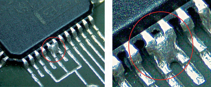
Troubleshooting Case Insights: Fine-Pitch QFN Challenges
Consider a high-density board with 0.4 mm pitch QFNs exhibiting inconsistent thermal pad wetting. Initial prints showed central voids due to excess paste migration. Switching to scooped apertures redistributed volume evenly, improving reflow fillet formation. Combined with adjusted snap-off, yields rose without changing paste or profile. Another scenario involved BGA haloing from stencil lift-off; electroformed stencils with coatings resolved it by enhancing snap-off cleanliness. These fixes highlight iterative validation using IPC J-STD-001J criteria for joint integrity. Engineers should log defect Pareto charts to prioritize stencil tweaks over reflow adjustments.
Conclusion
Advanced stencil printing techniques enable robust high-density SMT assembly by delivering precise, repeatable solder paste deposits. Focus on aperture innovations, parameter tuning, and standards compliance minimizes defects from print to reflow. Solder paste reflow optimization hinges on this upstream control, ensuring reliable electronics performance. Assembly teams benefit from proactive troubleshooting and process data to sustain yields. Adopting these practices positions engineers for success in evolving miniaturization trends. Prioritize stencil quality to unlock the full potential of dense PCB designs.
FAQs
Q1: What are the key benefits of advanced aperture designs in stencil printing for high density PCBs?
A1: Advanced aperture designs like U-shaped or scooped profiles improve solder paste release and volume control on fine-pitch pads. They reduce bridging risks and ensure uniform reflow by preventing excess center buildup on thermal pads. Fabrication via laser cutting or electroforming maintains wall smoothness, aligning with IPC-7525C guidelines. Troubleshooting shows these outperform rectangles for QFNs and BGAs, boosting yields in production.
Q2: How does stencil printing impact solder paste reflow optimization?
A2: Stencil printing determines deposit geometry, directly affecting reflow melting uniformity and joint formation. Consistent height and area prevent hotspots or voids during thermal profiling. Poor prints lead to defects like head-in-pillow, fixable by optimizing squeegee parameters. Engineers use SPI data to correlate prints with reflow outcomes, refining processes per IPC-7527 criteria for high-density success.
Q3: What common issues arise in stencil printing for high density PCBs and how to troubleshoot them?
A3: Bridging and insufficient paste top the list, often from mismatched aperture-to-pad ratios or worn stencils. Inspect via microscope or SPI, then adjust reductions or clean cycles. For slumping, verify paste rheology and humidity. Step stencils help mixed boards. Systematic DOE identifies root causes, ensuring reliable SMT assembly.
Q4: Why reference IPC standards in stencil printing processes?
A4: IPC standards like IPC-7525C and IPC-7527 provide proven guidelines for aperture design and print acceptability. They standardize practices across facilities, aiding troubleshooting and audits. Compliance verifies process capability for high-density PCBs, reducing variability in solder paste reflow optimization.
References
IPC-7525C — Stencil Design Guidelines. IPC, 2021
IPC-7527 — Requirements for Solder Paste Printing. IPC, 2012
IPC J-STD-001J — Requirements for Soldered Electrical and Electronic Assemblies. IPC, 2024


